All Activity
- Past hour
-
Thomas Garsia joined the community
- Today
-
SAMUEL BELLO joined the community
- Yesterday
-
hassan123 joined the community
-
Linga joined the community
-
vbsemi started following Should NMOS or PMOS be used as the upper tube of the circuit?
-
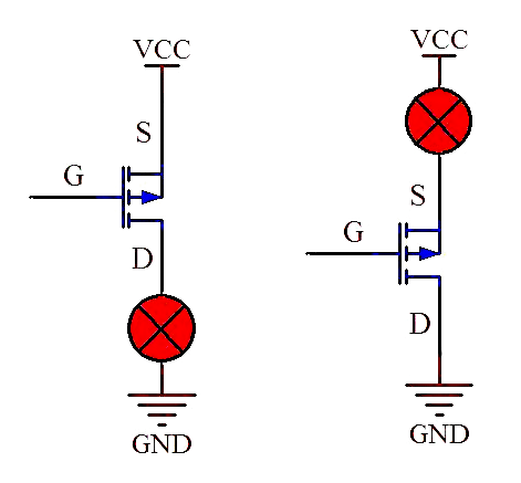
https://youtu.be/A7Q4pJbKY3k 有人说 NMOS 可以用作电路应用中的上管或下管。哪个更好?两者有什么区别? 众所周知,NMOS 和 PMOS 的电流方向相反,Vgs 具有一定的电压差。但是,NMOS 的 G 电位高于 S 电位 (5~10V),而 PMOS 的 S 电位高于 G 电位 (-5~-10V)。 这里,以 5V 的导通电压差为例,当使用 NMOS 作为下管时,S 极直接接地,将其固定到 5V 即可开启 G 极电压。 NMOS 如果用 NMOS 作为上管,D 极接正电源,S 极的电压不固定,则无法确定控制 NMOS 导通的 G 极电压,因为 S 极对地的电压有两种状态, MOS 管切断时为低电平,导通时接近高电平 VCC。但是,当 NMOS 用作上管时,控制电路会更加复杂。在这种情况下,必须使用隔离电源进行控制。改用 PMOS 会简单得多。 PMOS 使用 PMOS 作为上管时,S 极直接连接到电源 VCC,S 极电压是固定的,G 极电压只需要比 S 极低 5V 即可导通;同样,如果用 PMOS 作为下管,D 极接地, S 极电压不固定,无法确定控制极 G 极的电压,使用起来比较麻烦,需要隔离电压设计。 因此,在电路中通常使用 PMOS 作为上管,NMOS 作为下管。
-
Григорий Афанасьев joined the community
-
rixy2 joined the community
-
Hayes Vidal joined the community
- Last week
-
xxballer1995xx joined the community
-
hefleck400 started following Joshua Johnson
-
hefleck400 started following makesmovesonu82
-
hefleck400 started following topasew889
-
hefleck400 started following Hassan35
-
Guy marcel kalambay changed their profile photo
-
Aaron-Tecksay started following High-Speed Low power BLE 5.0 Bluetooth module TS-M1052
-
The TS-M1052 is a high-speed BLE 5.0 Bluetooth module that supports the Bluetooth BLE 5.0 protocol. It is known for its excellent stability and ultra-low power consumption. The module features Bluetooth serial port transparent transmission capability, and users can flexibly and freely modify parameters such as serial port baud rates and Bluetooth names using the provided AT commands. Model No.: TS-M1052 Features Bluetooth Version: BLE 5.0 Frequency Band: 2.402GHz-2.480GHz ISM band TX Power: -20dBm~+10dBm Receive Sensitivity: -96dBm Air Rate: 250Kbps/1Mbps/2Mbps Antenna: PCB Onboard Advise Range: 100m Memory: 32KB RAM Size: 26.7*13*2.3mm Pin/GPIO: 26/15 Power Supply: 1.8~3.6V Operating Temperature: -40℃~+85℃ Peripheral Interface: UART/I2C/ADC Serial Transparent Transmission Rate: BLE 20KB/s Applications Smart home Location tracking Intelligent educational equipment Measurement and monitoring system Industrial sensors and controls Medical equipment monitoring and wireless control
-
Mq Ms changed their profile photo
-
Raptor Power Systems changed their profile photo
-
Joshua Johnson changed their profile photo
-
Shahryar Pasyar changed their profile photo
-
Rully PP changed their profile photo
-
Mathieu Carbou changed their profile photo
-
Rajesh Bhor changed their profile photo
-
Mariel Coyoca changed their profile photo
-
Eric Seaman changed their profile photo
-
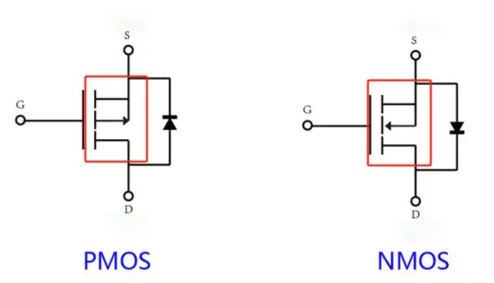
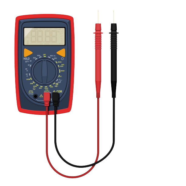
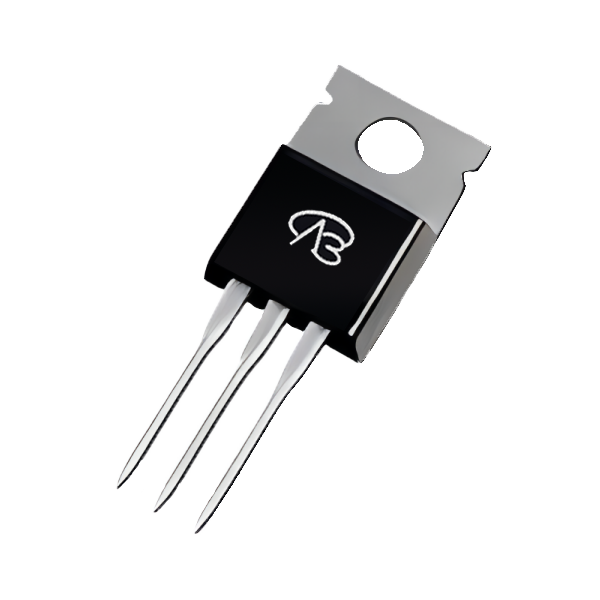
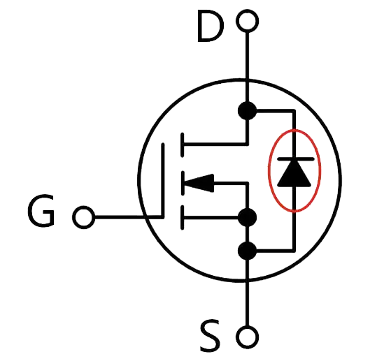
https://youtu.be/3e6fPoQ17wM 如何区分你手中的管子是N管还是P管? 首先,我们以增强MOS管为例。这是两者的电路符号: 您可以看到两个箭头的方向不一致。 这个箭头就是它的衬底,因为MOS管的内部衬底和源是连接在一起的。 NMOS和PMOS电路符号之间的最大区别在于其基板。NMOS的箭头指向闸门,而PMOS的箭头则指向闸门。 该箭头的方向与内部衬底与MOS管的通道逆温层之间的PN结方向有关。 其次,NMOS和PMOS的体二极管相反。 NMOS管的体二极管的阳极(即正极)连接到源极,PMOS的体二极管的阳极连接到漏极,体二极管的负极连接到源极。 那么,如何区分MOS管的三个引脚呢? 您可以使用万用表进行测试。下面简单说明一下。 拿一个封装为TO220的MOS管来说,它通常有一个散热片,散热片会连接到漏极。使用万用表测试哪个引脚可以连接到散热器,该散热器对应于漏极。 由于二极管的连接,漏极和源极之间存在二极管特性。 因此,当使用万用表测试漏极以及哪个引脚可以在正向和反向连接时,它就是源极。 剩下的就是大门了。 归纳起来,有两点: 1.NMOS二极管的正极一般接在源极上 2. 散热器连接到排水管
-
The TS-M1050 is a low-power Bluetooth module that operates on the Bluetooth 5.1 protocol, offering excellent stability and compatibility. The module supports direct Bluetooth system connections with seamless automatic reconnection, eliminating the need for an app. It features both momentary and latching modes of operation. Available with either a built-in or an external antenna option, it adapts to various project requirements. Model No.: TS-M1050 Features Bluetooth Version: BLE 5.1 Frequency Band: 2.402GHz-2.480GHz ISM band TX Power: -20dBm~+10Bm Receive Sensitivity: -95dBm Air Rate: 250Kbps/1Mbps/2Mbps Antenna: PCB Onboard / IPEX Antenna Advise Range: 50m Memory: 256KB FLASH+128KB RAM Size: 20*15*2.3mm Pin/GPIO: 21/13 Power Supply: 2.5~4.3V Operating Temperature: -40℃~+105℃ Peripheral Interface: UART/I2C/ADC Serial Transparent Transmission Rate: BLE 20KB/s Applications Smart door lock Car keyless entry Automatic induction switch
- Earlier
-
By positive flank you mean on the rising edge of the pulse or the pulse top? What is the nature of the pulse train? Voltage and pulse rates. "Need a circuit that can trigger a relay when movement or stop is detected on a axle." How does that relate to the pulse from the timer being on only 0.5 secs? Does that mean that if the pulse train is off for more than 0.5 seconds (axes stopped turning) the timer drops out resetting the relay? A retriggerable timer would stay on while it is constantly being reset else if not reset after 0.5 secs its output would go low. . For TTL logics datablade books see ebay.com Or even better Forrest Mims's book "Engineer's Note Book !! - A Handbook of Integrated Circuits Applications" is available online in pdf from: IC Book Dated but still the best book ever on ICs. The book has an NE555 circuit for missing pulse detection; which maybe what you need.
-
TS-M1037 Master-Slave Integration Features Bluetooth Version: BLE 5.2 Frequency Band: 2.402GHz-2.480GHz ISM band TX Power: -20dBm~+12Bm Receive Sensitivity: -96dBm Air Rate: 250Kbps/1Mbps/2Mbps Antenna: PCB Onboard / IPEX Antenna Advise Range: 100m CPU: Embedded 32-bits Processor Memory: 80KB RAM Size: 26.7*13*2.3mm Pin/GPIO: 21/13 Power Supply: 2~3.6V Operating Temperature: -40℃~+85℃ Peripheral Interface: UART/SPI/I2C/ADC Serial Transparent Transmission Rate: BLE 20KB/s Application Smart home Location tracking Intelligent educational equipment Measurement and monitoring system Industrial sensors and controls Medical equipment monitoring and wireless control
-
vbsemi started following Why do MOS tubes need to be connected in parallel with a diode?
-
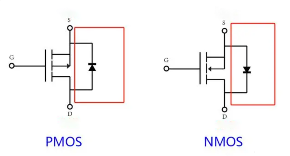
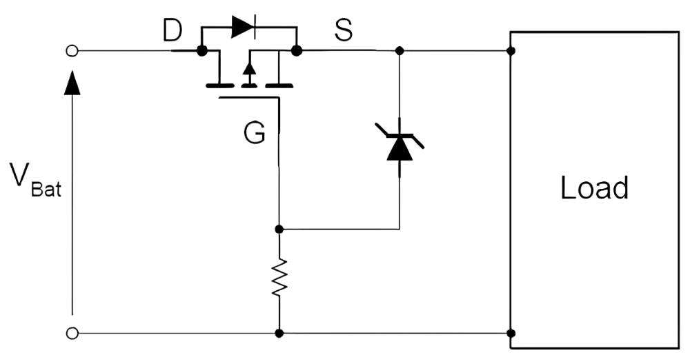
https://www.youtube.com/watch?v=pql2Ulae7mE MOS has a body diode connected in parallel between the D and S poles, so why is this diode connected in parallel? This starts with the process and structure of MOS. The diode is composed of a pair of PN junctions. The P-type region corresponds to the positive pole of the diode, the N-type region corresponds to the negative pole of the diode, and the PN junction is in the middle. SiO2 in the MOS tube itself is not conductive, so the driving pole G basically does not carry current. In addition to the three poles D, G, and S, there is also an intermediate pole, which is connected to the S pole, so in the circuit symbol of MOS, the arrow pointing to the channel N channel inside the MOS is connected to the S pole. In addition, the drain of the N-type region is connected to the middle P-type region and then to the source, which just forms a diode structure, so a diode is connected in parallel in the MOS symbol. What is the use of this body diode? In some scenarios, such as battery protection, after the lithium battery is over-discharged, the protection function will be turned on: turn off the discharge MOS. When the charger is plugged in, the MOS body diode is used to make the circuit conductive and the system work normally. However, in some scenarios, the existence of this diode is undesirable because it may cause leakage between the S pole and the D pole.
-
Thank you so much for sharing your guide on building a fun timelapse camera with the Xiao ESP32 S3 Sense. Your step-by-step instructions are clear and easy to follow, making the whole process feel exciting and achievable. I appreciate the effort you put into explaining both the hardware and software setup. Thanks again for this awesome project guide!
-
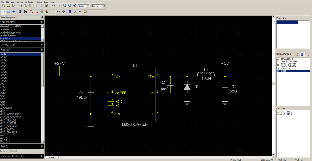
I’m working on a project where I need to step down 24V to a stable 5V with a load current of up to 1A. I’ve decided to use a buck converter based on the LM2675 IC. My schematic was made in DipTrace. Input: 24V (DC) Output: 5V / 1A Controller: LM2675 Switching Frequency: 260 kHz I’m planning to use two capacitors: Input Capacitor (C1): To smooth the input voltage and suppress noise. Output Capacitor (C2): To smooth the output voltage and minimize ripple. I have the following questions and concerns: Type and value of the input capacitor: I’m considering using a 100 µF electrolytic capacitor with low ESR, but I’ve heard that ceramic or polymer capacitors might be better for high-frequency applications. Which type would be optimal for input noise suppression? Type and value of the output capacitor: Given the need to minimize output ripple, should I use multiple low ESR ceramic capacitors or a single large electrolytic capacitor? Or perhaps a combination of both? Impact of switching frequency on capacitor selection: How does the 260 kHz switching frequency affect capacitor choice? Should this be a factor when determining capacitance? Temperature stability: The system will operate at elevated temperatures (up to 70°C). Which type of capacitor is best suited for these conditions? I’d appreciate any advice or suggestions! I’m especially interested in hearing from anyone who has experience with similar circuits. By the way, how do you like DipTrace 5? Has anyone tried working on it yet?
-
Hi! I did a lot of TTL logic back in the nineties but now I am lost. Need a circuit that can trigger a relay when movement or stop is detected on a axle. My approach is that the relay should stay active as long as the axle is turning. So, I decided to have the axle generate a pulse train. Next I need a timer that triggers on positive flank and then turns off the output after maybe half a second. If there is a new positive flank during this time the timer will restart. The reason I want it this way is that the axle might stop on a positive flank and not indicating a stop. As long as the axle is spinning the relay will stay active. Any ideas? Also: Once upon a time there was a TTL logics datablade book. Is such documentation still available?
-

False Turn-On in MOSFET Driving Circuit and Countermeasures
vbsemi posted a topic in Theory articles
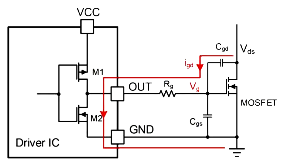
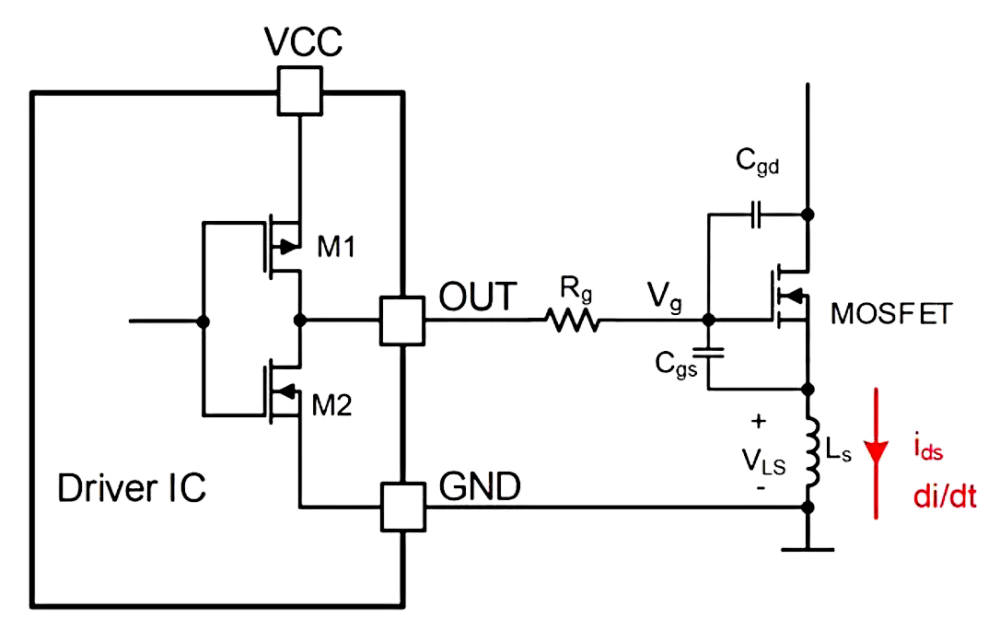
https://www.youtube.com/watch?v=PwOTTqUo9tA MOSFET is a switch controlled by gate voltage. When the gate voltage is greater than the turn-on threshold, the MOSFET is turned on; when the gate voltage is lower than the turn-on threshold, the MOSFET is turned off. In actual applications, due to the influence of other factors such as device and peripheral circuit parasitic parameters, the originally turned-off power device may be mistakenly turned on. Today, let's talk about the mistaken turn-on of MOSFET in the drive circuit and its countermeasures. Let's talk about two cases of mistaken turn-on: mistaken turn-on caused by Miller effect and mistaken turn-on caused by parasitic inductance. False turn-on caused by Miller effect When the MOSFET is turned off and then turned on, the Vds voltage (the maximum voltage that can be applied between the drain and the source) rises rapidly to produce a high dv/dt (the rate of change of the drain-source voltage during the switching transient), thereby generating a displacement current (igd) in the capacitor Cgd (Miller capacitor). This displacement current will generate a voltage spike after flowing through . If this voltage spike exceeds the turn-on threshold of the MOSFET, the MOSFET will be turned on, causing the circuit to be turned on or even damaged. Another type of false turn-on is caused by parasitic inductance on the line. As shown in the figure below, Ls is the parasitic inductance on the source of the MOSFET. When the MOSFET is turned off quickly, the current decreases rapidly to produce a high di/dt, and then a negative voltage (VLS) is generated across the two ends of the parasitic inductance. If this VLS voltage exceeds the gate threshold of the MOSFET, the MOSFET will be turned on by mistake. So, what methods do we have to deal with the phenomenon of MOSFET being turned on by mistake? 1. Adjust the gate drive resistor and capacitor The turn-on/off speed of the MOSFET can be adjusted by adjusting the size of the gate drive resistor and capacitor: increase the gate drive resistor and capacitor to slow down the turn-on/off speed of the MOSFET, reduce dv/dt (di/dt) and thus reduce the gate voltage spike. 2. Add a transistor A transistor can be placed near the gate of the power tube to prevent false opening during the shutdown period, effectively suppressing the false gate opening caused by the Miller effect. 3. Use an anti-parallel diode The current in the inductor can disappear through the diode loop, thereby avoiding the generation of reverse potential.-
- mosfet
- semiconductor
-
(and 2 more)
Tagged with:
-
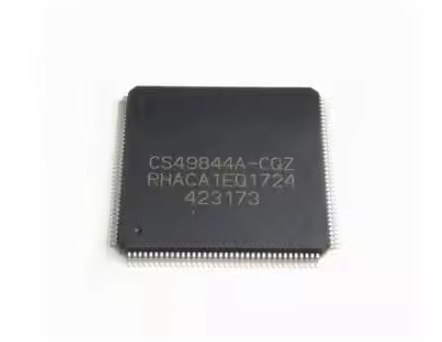
Class-D audio amplifiers are known for their efficiency and compact design, making them ideal for modern audio systems where power efficiency and space are critical. The CS49844A-CQZ offers advanced features such as high output power, low distortion, and integrated protection circuits, making it an excellent choice for building a robust audio amplifier. Objectives: Design a high-efficiency Class-D audio amplifier using the CS49844A-CQZ. Achieve high audio fidelity with minimal distortion and noise. Optimize the system for power efficiency and thermal management. Evaluate the amplifier’s performance in various audio applications. Materials and Methods: Components Required: CS49844A-CQZ IC (datasheet required for pin configuration and operational details). Passive components: resistors, capacitors, and inductors for filter networks and compensation. Audio source (e.g., audio DAC or preamp module). Speaker(s) matching the amplifier’s output specifications. Power supply suitable for the amplifier's voltage and current requirements. Heat sink (if needed, based on thermal calculations). System Design: Amplifier Circuit Design: Refer to the CS49844A-CQZ datasheet for the recommended application circuit and configuration. Design the input stage to interface with the audio source, ensuring proper signal conditioning. Configure the feedback network and output stage for optimal performance, including setting gain and compensation components. Power Supply and Protection: Choose a power supply that matches the voltage and current requirements of the CS49844A-CQZ. Implement appropriate power filtering and decoupling to minimize noise and ensure stable operation. Utilize the IC’s built-in protection features (over-temperature, over-current) and add external components if necessary. PCB Design and Assembly: Design a printed circuit board (PCB) layout that minimizes signal interference and maximizes thermal dissipation. Assemble the components carefully, paying attention to the placement of decoupling capacitors and the heat sink. Testing and Calibration: Connect the amplifier to an audio source and speaker system. Measure output power, distortion, and efficiency using appropriate audio test equipment. Fine-tune the circuit to achieve the desired audio performance and ensure reliable operation under various conditions. Results: The project will demonstrate the capabilities of the CS49844A-CQZ in delivering high-quality audio amplification with high efficiency. Results will include audio performance metrics such as total harmonic distortion (THD), signal-to-noise ratio (SNR), and power efficiency. The design’s ability to maintain performance while minimizing heat and power consumption will be highlighted. Conclusion: Building a Class-D audio amplifier system with the CS49844A-CQZ showcases the benefits of modern audio amplification technologies in achieving high fidelity and efficiency. The project illustrates the practical application of high-performance audio ICs in creating advanced audio solutions for both consumer and professional use. References: CS49844A-CQZ datasheet and technical documentation. Application notes on Class-D amplifier design and optimization. Audio amplifier design guidelines and best practices.
-
This project is based on the Forlinx Embedded OKMX8MP-C development board, which has a virtual machine ported. It is necessary to install the required packages on the development board and ensure that the board is connected to the network. 01 Logging into the OKMX8MP-C Development Board Connect the Type-C cable to the Debug port and select eMMC as the boot mode (i.e., set mode selection switch 2 to “on” and all others to “off”). After booting, log in using the root account. 02 Modifying the pip Source To speed up the installation process, it is necessary to modify the pip source: Add the followings: 03 Installing the Python venv Environment First, install the python3-venv package: apt install python3-venv Once installed successfully, create a directory named yolo (or any name of choice) and enter this directory to set up the Python 3 environment: Create the yolo directory (the directory name can be taken by yourself), and enter the directory to install the python3 environment: Execute the following figure: Activate the Python 3 venv environment: If activation is successful, it will display the following: 04 Installing Ultralytics Ultralytics YOLOv8 is based on cutting-edge deep learning and computer vision technologies, offering unparalleled performance in speed and accuracy. Its streamlined design makes it suitable for various applications and easily adaptable to different hardware platforms, from edge devices to cloud API. To install it, use the following command: Be patient while the installation completes: Once the installation is successful: 05 Testing the Installation Use the following command to test the setup. The image link in source can be replaced with another link: During this process, the model and image will be downloaded, so patience is required. After successful execution, the results will be generated in the runs/detect/predict* directory. The results can be copied to a Windows computer using the scp command. In the cmd terminal, execute the following command: If the output can be recognized, it indicates that the YOLO environment is functioning correctly. It is the process of setting up the YOLO environment on the Forlinx Embedded OKMX8MP-C development board. Hope it is useful.
-
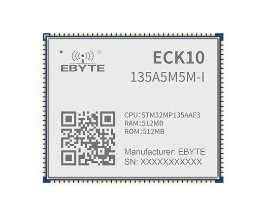
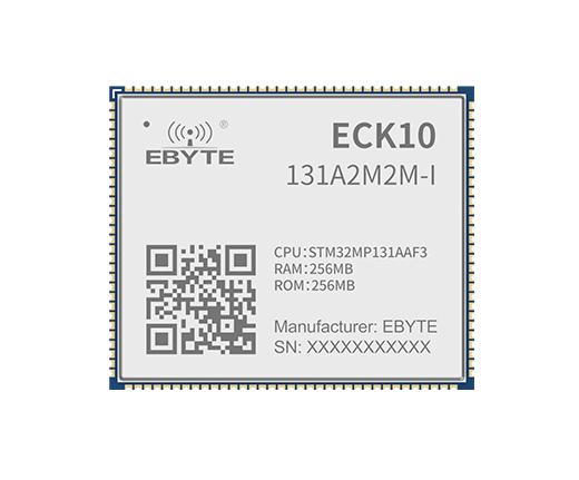
ECK10 sereis Memory Capacity low power System on Module (SoM) CPU module Industrial Computing Based on ST's cost-effective MPU design Discover the EBYTE ECK10 series CPU modules, Low-power System-on-Module (SoM). Based on ST's cost-effective MPU design which is STM32MP13 series processor launched by STMicroelectronics , it is designed for industrial computing, automation control and IoT applications. Learn more about industrial computing applications and optimize your system design.Talk to us online for a technical consultation . [Processor model]:STM32MP131AAF3 [Processor Core]:Single Core [Processor frequency]: 650MHz [Product size]:38*32*3.1mm [Introduction]:ECK10-131A2M2M-I /ECK10-135A5M5M-I CPU module is carefully designed based on the STM32MP13 series processor launched by STMicroelectronics. It is a low-cost, low-power, cost-effective, and highly reliable embedded core board that uses stamp hole connections. The ECK10-13xA series core board is centered on the STM32MP13 series processor, and the power supply circuit, DDR3L memory circuit, NAND FLASH storage circuit, and Gigabit Ethernet PHY circuit are designed on the board to minimize the difficulty and cost of user baseboard design.
-
Ever wanted to capture the beauty of a sunset, the hustle and bustle of a busy street, or the growth of a plant in a fun and creative way? With the Xiao ESP32 S3 Sense, you can build your very own timelapse camera! This tiny yet powerful board is perfect for capturing stunning timelapse videos. Let’s dive into this exciting project step-by-step. 🚀 Materials Needed 🛠️ Xiao ESP32 S3 Sense: The brain of our project. Camera module: Included with the Xiao ESP32 S3 Sense. MicroSD card: For storing your amazing timelapse photos (formatted to FAT32). USB Type-C cable: To power up your board. Power source: A battery or USB power bank for portability. Get PCBs for Your Projects Manufactured You must check out PCBWAY for ordering PCBs online for cheap! You get 10 good-quality PCBs manufactured and shipped to your doorstep for cheap. You will also get a discount on shipping on your first order. Upload your Gerber files onto PCBWAY to get them manufactured with good quality and quick turnaround time. PCBWay now could provide a complete product solution, from design to enclosure production. Check out their online Gerber viewer function. With reward points, you can get free stuff from their gift shop. Also, check out this useful blog on PCBWay Plugin for KiCad from here. Using this plugin, you can directly order PCBs in just one click after completing your design in KiCad. Step 1: Hardware Setup 🔧 Connect the Camera Module: Attach the camera module to the Xiao ESP32 S3 Sense board. Make sure it’s snug and secure. Insert the MicroSD Card: Pop the formatted MicroSD card into the slot on the Xiao ESP32 S3 Sense. Power the Board: Plug in the Xiao ESP32 S3 Sense using the USB Type-C cable. You can use a battery or a USB power bank if you want to take your camera on the go. Step 2: Software Setup 💻 Install Arduino IDE: If you haven’t already, download and install the Arduino IDE from the official website. Add ESP32 Board to Arduino IDE: Open Arduino IDE and go to File > Preferences. In the “Additional Board Manager URLs” field, add: https://raw.githubusercontent.com/espressif/arduino-esp32/gh-pages/package_esp32_index.json. Go to Tools > Board > Board Manager, search for “ESP32”, and install the ESP32 board package. Select the Xiao ESP32 S3 Sense Board: Go to Tools > Board and select Xiao ESP32 S3 Sense. Choose the correct port from Tools > Port. Step 3: Coding 👨💻 Install Required Libraries: Open Arduino IDE and go to examples and ESP32 CAM then Camera Web Server: Just replace the complete ino file with the following code Arduino Code: #include "esp_camera.h" #include "FS.h" #include "SD.h" #include "SPI.h" #define CAMERA_MODEL_XIAO_ESP32S3 // Has PSRAM #include "camera_pins.h" unsigned long lastCaptureTime = 0; // Last shooting time int imageCount = 1; // File Counter bool camera_sign = false; // Check camera status bool sd_sign = false; // Check sd status // Save pictures to SD card void photo_save(const char * fileName) { // Take a photo camera_fb_t *fb = esp_camera_fb_get(); if (!fb) { Serial.println("Failed to get camera frame buffer"); return; } // Save photo to file writeFile(SD, fileName, fb->buf, fb->len); // Release image buffer esp_camera_fb_return(fb); Serial.println("Photo saved to file"); } // SD card write file void writeFile(fs::FS &fs, const char * path, uint8_t * data, size_t len){ Serial.printf("Writing file: %s\n", path); File file = fs.open(path, FILE_WRITE); if(!file){ Serial.println("Failed to open file for writing"); return; } if(file.write(data, len) == len){ Serial.println("File written"); } else { Serial.println("Write failed"); } file.close(); } void setup() { Serial.begin(115200); while(!Serial); // When the serial monitor is turned on, the program starts to execute camera_config_t config; config.ledc_channel = LEDC_CHANNEL_0; config.ledc_timer = LEDC_TIMER_0; config.pin_d0 = Y2_GPIO_NUM; config.pin_d1 = Y3_GPIO_NUM; config.pin_d2 = Y4_GPIO_NUM; config.pin_d3 = Y5_GPIO_NUM; config.pin_d4 = Y6_GPIO_NUM; config.pin_d5 = Y7_GPIO_NUM; config.pin_d6 = Y8_GPIO_NUM; config.pin_d7 = Y9_GPIO_NUM; config.pin_xclk = XCLK_GPIO_NUM; config.pin_pclk = PCLK_GPIO_NUM; config.pin_vsync = VSYNC_GPIO_NUM; config.pin_href = HREF_GPIO_NUM; config.pin_sscb_sda = SIOD_GPIO_NUM; config.pin_sscb_scl = SIOC_GPIO_NUM; config.pin_pwdn = PWDN_GPIO_NUM; config.pin_reset = RESET_GPIO_NUM; config.xclk_freq_hz = 20000000; config.frame_size = FRAMESIZE_UXGA; config.pixel_format = PIXFORMAT_JPEG; // for streaming config.grab_mode = CAMERA_GRAB_WHEN_EMPTY; config.fb_location = CAMERA_FB_IN_PSRAM; config.jpeg_quality = 12; config.fb_count = 1; // if PSRAM IC present, init with UXGA resolution and higher JPEG quality // for larger pre-allocated frame buffer. if(config.pixel_format == PIXFORMAT_JPEG){ if(psramFound()){ config.jpeg_quality = 10; config.fb_count = 2; config.grab_mode = CAMERA_GRAB_LATEST; } else { // Limit the frame size when PSRAM is not available config.frame_size = FRAMESIZE_SVGA; config.fb_location = CAMERA_FB_IN_DRAM; } } else { // Best option for face detection/recognition config.frame_size = FRAMESIZE_240X240; #if CONFIG_IDF_TARGET_ESP32S3 config.fb_count = 2; #endif } // camera init esp_err_t err = esp_camera_init(&config); if (err != ESP_OK) { Serial.printf("Camera init failed with error 0x%x", err); return; } camera_sign = true; // Camera initialization check passes // Initialize SD card if(!SD.begin(21)){ Serial.println("Card Mount Failed"); return; } uint8_t cardType = SD.cardType(); // Determine if the type of SD card is available if(cardType == CARD_NONE){ Serial.println("No SD card attached"); return; } Serial.print("SD Card Type: "); if(cardType == CARD_MMC){ Serial.println("MMC"); } else if(cardType == CARD_SD){ Serial.println("SDSC"); } else if(cardType == CARD_SDHC){ Serial.println("SDHC"); } else { Serial.println("UNKNOWN"); } sd_sign = true; // sd initialization check passes Serial.println("Photos will begin in one minute, please be ready."); } void loop() { // Camera & SD available, start taking pictures if(camera_sign && sd_sign){ // Get the current time unsigned long now = millis(); //If it has been more than 1 minute since the last shot, take a picture and save it to the SD card if ((now - lastCaptureTime) >= 60000) { char filename[32]; sprintf(filename, "/image%d.jpg", imageCount); photo_save(filename); Serial.printf("Saved picture:%s\n", filename); Serial.println("Photos will begin in one minute, please be ready."); imageCount++; lastCaptureTime = now; } } } If you want you can change the time interval. Step 4: Upload and Test 🚀 Upload the Code: Connect your Xiao ESP32 S3 Sense to your computer, Select the correct COM port, and upload the code using the Arduino IDE. Test the Camera: Once the code is uploaded, the camera will start capturing images at regular intervals and saving them to the MicroSD card. You can open the serial terminal and look for the response. Step 5: Create the Timelapse Video 🎥 Retrieve Images: Remove the MicroSD card from the Xiao ESP32 S3 Sense and transfer the images to your computer. Compile the Timelapse Video: Use video editing software like Adobe Premiere Pro, Final Cut Pro, or free alternatives like OpenShot or Shotcut to compile the images into a timelapse video. Or you can simply use a python script to do that. Here is the Python code to convert jpeg to video: import cv2 import numpy as np import time import os nframes = 500 interval = 0.5 fps=100 print("XIAO ESP32 S3 Sense TimeLapser") # Define the path to the photos folder photos_path = "photos/" # Get the list of photo filenames photos = os.listdir(photos_path) # Sort the photos by name photos.sort() # Create a video writer object video = cv2.VideoWriter("video.avi", cv2.VideoWriter_fourcc(*"MJPG"), 100, (800, 600)) # Loop through the photos for photo in photos: # Read the photo as an image image = cv2.imread(photos_path + photo) # Resize the image to fit the video frame image = cv2.resize(image, (800, 600)) # Write the image to the video video.write(image) # Release the video writer object video.release() print("Video Build Completed") Final Output from Xiao ESP32 S3 Sense: Conclusion 🎉 Congratulations! You’ve successfully built a small timelapse camera using the Xiao ESP32 S3 Sense. This project can be expanded further by adding features like remote control, different capture intervals, or even uploading images to the cloud. Feel free to share your timelapse videos and any modifications you make to this project. Happy building! 🛠️
-
Also had a hard time to find the component, but finally I found it! It's a component by SG-Micro, the model is SGM2036-3.3. It's a 3.3V Voltage Linear Regulator. You can find the datasheet here: https://www.sg-micro.com/product/SGM2036
-
The TS-M1036 is a high-speed, master-slave integrated BLE 5.2 Bluetooth module, known for its exceptional stability and ultra-low power consumption. The module comes with a default Bluetooth serial port transparent transmission feature, and users can modify parameters such as serial port baud rates and device names using the provided AT commands, ensuring flexible and easy operation. This module excels with its excellent stability, ultra-low cost, minimal power consumption, and high reception sensitivity, making it suitable for a wide range of customer development projects. Model No.: TS-M1036 Features Bluetooth Version: BLE 5.2 Frequency Band: 2.402GHz-2.480GHz ISM band TX Power: -20dBm~+12Bm Receive Sensitivity: -96dBm Air Rate: 250Kbps/1Mbps/2Mbps Antenna: PCB Onboard Advise Range: 100m CPU: Embedded 32-bits Processor Memory: 80KB RAM Size: 17*13*2.3mm Pin/GPIO: 21/13 Power Supply: 2~3.6V Operating Temperature: -40℃~+85℃ Peripheral Interface: UART/SPI/I2C/ADC Serial Transparent Transmission Rate: BLE 20KB/s Applications Smart home Location tracking Intelligent educational equipment Measurement and monitoring system Industrial sensors and controls Medical equipment monitoring and wireless control
-
The TS-M1035 is a high-speed BLE 5.1 Bluetooth module that supports serial port transparent transmission, master-slave mode, and AT commands. Users can easily modify parameters such as serial port baud rates and device names using the provided AT commands, offering flexible and straightforward operation. This module boasts excellent stability, ultra-low cost, and high reception sensitivity. It is available with either a built-in or an external antenna option, catering to various project needs. Model No.: TS-M1035 Features Bluetooth Version: BLE 5.1 Frequency Band: 2.402GHz-2.480GHz ISM band TX Power: -20dBm~+10Bm Receive Sensitivity: -95dBm Air Rate: 250Kbps/1Mbps/2Mbps Antenna: PCB Onboard / IPEX Antenna Advise Range: 80m Memory: 48KB RAM Size: 20*15*1.5mm Pin/GPIO: 16/12 Power Supply: 2.5~4.3V Operating Temperature: -40℃~+105℃ Peripheral Interface: UART/SPI/I2C/ADC Serial Transparent Transmission Rate: BLE 20KB/s Applications Smart home Location tracking Bluetooth electronic scale Intelligent educational equipment Vehicle testing equipment Measurement and monitoring system Bluetooth wireless data transmission Industrial sensors and controls Medical equipment monitoring and wireless control
-
MIPI-CSI is a common camera interface in embedded systems or mobile devices, enabling high-speed image data transfer. The latest OK3576-C development board from Forlinx Embedded offers a wealth of resource interfaces, including support for 5 x CSI-2 , meaning it can support up to five camera inputs simultaneously. This article introduces the Camera path of RK3576 processor and how to configure different output formats of MIPI-CSI camera through OK3576-C development board. 01. RK3576 Camera Channels If there is only one camera access, turn on only rkispx_vir0 . Please note: vicap and isp do not have a direct correspondence; The relationships between different vir0/vir1 channels are essentially the same hardware being multiplexed, with the same effect. When using multiple cameras, configure them using 0, 1, 2, etc., as much as possible. The hardware channel diagram is as follows: There is one dcphy interface and two dphy interfaces. The connection paths are as follows: Single Camera (connected to one dphy): Dual Cameras (connected to two dphys) Three Cameras (connected to dcphy and two dphys) Five Cameras (connected to dcphy and two split dphys) Camera Channel Connection Diagram: (Note: For RGB data input, it is also necessary to connect to rkisp_virx) 02. Sensor Link Scenarios for Different Platforms yuv422/rgb888 input There are three common scenarios for yuv422/rgb888 input: Cameras with Built-in isp or External isp. Enter yuv422 format; HDMI to MIPI CSI Input. Common chips like rk628d/f,lt6911xxx, etc., typically convert yuv422, but rgb888 format is also possible; Multiple ahd and serdes. A single mipi port can support up to four virtual channels. For these scenarios, an isp is not required, and the connection only needs to go to cif. Thus, the link is: The isp node can be disabled. The X varies depending on the platform and hardware connections. The node used for capturing images is the first video node corresponding to rkcif_mipi_lvdsX. This can be viewed using media-ctl to check the topology. For example, on the OK3576-C development board with an OV5645 camera, it is mounted on the media1 node. root@ok3576-buildroot:/# media-ctl -p -d /dev/media1 Media controller API version 6.1.57 driver rkcif model rkcif-mipi-lvds1 serial bus info platform:rkcif-mipi-lvds1 hw revision 0x0 driver version 6.1.57 Device topology - entity 1: stream_cif_mipi_id0 (1 pad, 11 links) type Node subtype V4L flags 0 device node name /dev/video11 pad0: Sink <- "rockchip-mipi-csi2":1 [ENABLED] <- "rockchip-mipi-csi2":2 [] <- "rockchip-mipi-csi2":3 [] <- "rockchip-mipi-csi2":4 [] <- "rockchip-mipi-csi2":5 [] <- "rockchip-mipi-csi2":6 [] <- "rockchip-mipi-csi2":7 [] <- "rockchip-mipi-csi2":8 [] <- "rockchip-mipi-csi2":9 [] <- "rockchip-mipi-csi2":10 [] <- "rockchip-mipi-csi2":11 [] - entity 5: stream_cif_mipi_id1 (1 pad, 11 links) type Node subtype V4L flags 0 device node name /dev/video12 pad0: Sink <- "rockchip-mipi-csi2":1 [] <- "rockchip-mipi-csi2":2 [ENABLED] <- "rockchip-mipi-csi2":3 [] <- "rockchip-mipi-csi2":4 [] <- "rockchip-mipi-csi2":5 [] <- "rockchip-mipi-csi2":6 [] <- "rockchip-mipi-csi2":7 [] <- "rockchip-mipi-csi2":8 [] <- "rockchip-mipi-csi2":9 [] <- "rockchip-mipi-csi2":10 [] <- "rockchip-mipi-csi2":11 [] - entity 9: stream_cif_mipi_id2 (1 pad, 11 links) type Node subtype V4L flags 0 device node name /dev/video13 pad0: Sink <- "rockchip-mipi-csi2":1 [] <- "rockchip-mipi-csi2":2 [] <- "rockchip-mipi-csi2":3 [ENABLED] <- "rockchip-mipi-csi2":4 [] <- "rockchip-mipi-csi2":5 [] <- "rockchip-mipi-csi2":6 [] <- "rockchip-mipi-csi2":7 [] <- "rockchip-mipi-csi2":8 [] <- "rockchip-mipi-csi2":9 [] <- "rockchip-mipi-csi2":10 [] <- "rockchip-mipi-csi2":11 [] - entity 13: stream_cif_mipi_id3 (1 pad, 11 links) type Node subtype V4L flags 0 device node name /dev/video14 pad0: Sink <- "rockchip-mipi-csi2":1 [] <- "rockchip-mipi-csi2":2 [] <- "rockchip-mipi-csi2":3 [] <- "rockchip-mipi-csi2":4 [ENABLED] <- "rockchip-mipi-csi2":5 [] <- "rockchip-mipi-csi2":6 [] <- "rockchip-mipi-csi2":7 [] <- "rockchip-mipi-csi2":8 [] <- "rockchip-mipi-csi2":9 [] <- "rockchip-mipi-csi2":10 [] <- "rockchip-mipi-csi2":11 [] - entity 17: rkcif_scale_ch0 (1 pad, 11 links) type Node subtype V4L flags 0 device node name /dev/video15 pad0: Sink <- "rockchip-mipi-csi2":1 [] <- "rockchip-mipi-csi2":2 [] <- "rockchip-mipi-csi2":3 [] <- "rockchip-mipi-csi2":4 [] <- "rockchip-mipi-csi2":5 [ENABLED] <- "rockchip-mipi-csi2":6 [] <- "rockchip-mipi-csi2":7 [] <- "rockchip-mipi-csi2":8 [] <- "rockchip-mipi-csi2":9 [] <- "rockchip-mipi-csi2":10 [] <- "rockchip-mipi-csi2":11 [] - entity 21: rkcif_scale_ch1 (1 pad, 11 links) type Node subtype V4L flags 0 device node name /dev/video16 pad0: Sink <- "rockchip-mipi-csi2":1 [] <- "rockchip-mipi-csi2":2 [] <- "rockchip-mipi-csi2":3 [] <- "rockchip-mipi-csi2":4 [] <- "rockchip-mipi-csi2":5 [] <- "rockchip-mipi-csi2":6 [ENABLED] <- "rockchip-mipi-csi2":7 [] <- "rockchip-mipi-csi2":8 [] <- "rockchip-mipi-csi2":9 [] <- "rockchip-mipi-csi2":10 [] <- "rockchip-mipi-csi2":11 [] - entity 25: rkcif_scale_ch2 (1 pad, 11 links) type Node subtype V4L flags 0 device node name /dev/video17 pad0: Sink <- "rockchip-mipi-csi2":1 [] <- "rockchip-mipi-csi2":2 [] <- "rockchip-mipi-csi2":3 [] <- "rockchip-mipi-csi2":4 [] <- "rockchip-mipi-csi2":5 [] <- "rockchip-mipi-csi2":6 [] <- "rockchip-mipi-csi2":7 [ENABLED] <- "rockchip-mipi-csi2":8 [] <- "rockchip-mipi-csi2":9 [] <- "rockchip-mipi-csi2":10 [] <- "rockchip-mipi-csi2":11 [] - entity 29: rkcif_scale_ch3 (1 pad, 11 links) type Node subtype V4L flags 0 device node name /dev/video18 pad0: Sink <- "rockchip-mipi-csi2":1 [] <- "rockchip-mipi-csi2":2 [] <- "rockchip-mipi-csi2":3 [] <- "rockchip-mipi-csi2":4 [] <- "rockchip-mipi-csi2":5 [] <- "rockchip-mipi-csi2":6 [] <- "rockchip-mipi-csi2":7 [] <- "rockchip-mipi-csi2":8 [ENABLED] <- "rockchip-mipi-csi2":9 [] <- "rockchip-mipi-csi2":10 [] <- "rockchip-mipi-csi2":11 [] - entity 33: rkcif_tools_id0 (1 pad, 11 links) type Node subtype V4L flags 0 device node name /dev/video19 pad0: Sink <- "rockchip-mipi-csi2":1 [] <- "rockchip-mipi-csi2":2 [] <- "rockchip-mipi-csi2":3 [] <- "rockchip-mipi-csi2":4 [] <- "rockchip-mipi-csi2":5 [] <- "rockchip-mipi-csi2":6 [] <- "rockchip-mipi-csi2":7 [] <- "rockchip-mipi-csi2":8 [] <- "rockchip-mipi-csi2":9 [ENABLED] <- "rockchip-mipi-csi2":10 [] <- "rockchip-mipi-csi2":11 [] - entity 37: rkcif_tools_id1 (1 pad, 11 links) type Node subtype V4L flags 0 device node name /dev/video20 pad0: Sink <- "rockchip-mipi-csi2":1 [] <- "rockchip-mipi-csi2":2 [] <- "rockchip-mipi-csi2":3 [] <- "rockchip-mipi-csi2":4 [] <- "rockchip-mipi-csi2":5 [] <- "rockchip-mipi-csi2":6 [] <- "rockchip-mipi-csi2":7 [] <- "rockchip-mipi-csi2":8 [] <- "rockchip-mipi-csi2":9 [] <- "rockchip-mipi-csi2":10 [ENABLED] <- "rockchip-mipi-csi2":11 [] - entity 41: rkcif_tools_id2 (1 pad, 11 links) type Node subtype V4L flags 0 device node name /dev/video21 pad0: Sink <- "rockchip-mipi-csi2":1 [] <- "rockchip-mipi-csi2":2 [] <- "rockchip-mipi-csi2":3 [] <- "rockchip-mipi-csi2":4 [] <- "rockchip-mipi-csi2":5 [] <- "rockchip-mipi-csi2":6 [] <- "rockchip-mipi-csi2":7 [] <- "rockchip-mipi-csi2":8 [] <- "rockchip-mipi-csi2":9 [] <- "rockchip-mipi-csi2":10 [] <- "rockchip-mipi-csi2":11 [ENABLED] - entity 45: rockchip-mipi-csi2 (12 pads, 122 links) type V4L2 subdev subtype Unknown flags 0 device node name /dev/v4l-subdev1 pad0: Sink [fmt:UYVY8_2X8/1920x1080 field:none colorspace:srgb crop.bounds:(0,0)/1920x1080 crop:(0,0)/1920x1080] <- "rockchip-csi2-dphy0":1 [ENABLED] pad1: Source -> "stream_cif_mipi_id0":0 [ENABLED] -> "stream_cif_mipi_id1":0 [] -> "stream_cif_mipi_id2":0 [] -> "stream_cif_mipi_id3":0 [] -> "rkcif_scale_ch0":0 [] -> "rkcif_scale_ch1":0 [] -> "rkcif_scale_ch2":0 [] -> "rkcif_scale_ch3":0 [] -> "rkcif_tools_id0":0 [] -> "rkcif_tools_id1":0 [] -> "rkcif_tools_id2":0 [] pad2: Source -> "stream_cif_mipi_id0":0 [] -> "stream_cif_mipi_id1":0 [ENABLED] -> "stream_cif_mipi_id2":0 [] -> "stream_cif_mipi_id3":0 [] -> "rkcif_scale_ch0":0 [] -> "rkcif_scale_ch1":0 [] -> "rkcif_scale_ch2":0 [] -> "rkcif_scale_ch3":0 [] -> "rkcif_tools_id0":0 [] -> "rkcif_tools_id1":0 [] -> "rkcif_tools_id2":0 [] pad3: Source -> "stream_cif_mipi_id0":0 [] -> "stream_cif_mipi_id1":0 [] -> "stream_cif_mipi_id2":0 [ENABLED] -> "stream_cif_mipi_id3":0 [] -> "rkcif_scale_ch0":0 [] -> "rkcif_scale_ch1":0 [] -> "rkcif_scale_ch2":0 [] -> "rkcif_scale_ch3":0 [] -> "rkcif_tools_id0":0 [] -> "rkcif_tools_id1":0 [] -> "rkcif_tools_id2":0 [] pad4: Source -> "stream_cif_mipi_id0":0 [] -> "stream_cif_mipi_id1":0 [] -> "stream_cif_mipi_id2":0 [] -> "stream_cif_mipi_id3":0 [ENABLED] -> "rkcif_scale_ch0":0 [] -> "rkcif_scale_ch1":0 [] -> "rkcif_scale_ch2":0 [] -> "rkcif_scale_ch3":0 [] -> "rkcif_tools_id0":0 [] -> "rkcif_tools_id1":0 [] -> "rkcif_tools_id2":0 [] pad5: Source -> "stream_cif_mipi_id0":0 [] -> "stream_cif_mipi_id1":0 [] -> "stream_cif_mipi_id2":0 [] -> "stream_cif_mipi_id3":0 [] -> "rkcif_scale_ch0":0 [ENABLED] -> "rkcif_scale_ch1":0 [] -> "rkcif_scale_ch2":0 [] -> "rkcif_scale_ch3":0 [] -> "rkcif_tools_id0":0 [] -> "rkcif_tools_id1":0 [] -> "rkcif_tools_id2":0 [] pad6: Source -> "stream_cif_mipi_id0":0 [] -> "stream_cif_mipi_id1":0 [] -> "stream_cif_mipi_id2":0 [] -> "stream_cif_mipi_id3":0 [] -> "rkcif_scale_ch0":0 [] -> "rkcif_scale_ch1":0 [ENABLED] -> "rkcif_scale_ch2":0 [] -> "rkcif_scale_ch3":0 [] -> "rkcif_tools_id0":0 [] -> "rkcif_tools_id1":0 [] -> "rkcif_tools_id2":0 [] pad7: Source -> "stream_cif_mipi_id0":0 [] -> "stream_cif_mipi_id1":0 [] -> "stream_cif_mipi_id2":0 [] -> "stream_cif_mipi_id3":0 [] -> "rkcif_scale_ch0":0 [] -> "rkcif_scale_ch1":0 [] -> "rkcif_scale_ch2":0 [ENABLED] -> "rkcif_scale_ch3":0 [] -> "rkcif_tools_id0":0 [] -> "rkcif_tools_id1":0 [] -> "rkcif_tools_id2":0 [] pad8: Source -> "stream_cif_mipi_id0":0 [] -> "stream_cif_mipi_id1":0 [] -> "stream_cif_mipi_id2":0 [] -> "stream_cif_mipi_id3":0 [] -> "rkcif_scale_ch0":0 [] -> "rkcif_scale_ch1":0 [] -> "rkcif_scale_ch2":0 [] -> "rkcif_scale_ch3":0 [ENABLED] -> "rkcif_tools_id0":0 [] -> "rkcif_tools_id1":0 [] -> "rkcif_tools_id2":0 [] pad9: Source -> "stream_cif_mipi_id0":0 [] -> "stream_cif_mipi_id1":0 [] -> "stream_cif_mipi_id2":0 [] -> "stream_cif_mipi_id3":0 [] -> "rkcif_scale_ch0":0 [] -> "rkcif_scale_ch1":0 [] -> "rkcif_scale_ch2":0 [] -> "rkcif_scale_ch3":0 [] -> "rkcif_tools_id0":0 [ENABLED] -> "rkcif_tools_id1":0 [] -> "rkcif_tools_id2":0 [] pad10: Source -> "stream_cif_mipi_id0":0 [] -> "stream_cif_mipi_id1":0 [] -> "stream_cif_mipi_id2":0 [] -> "stream_cif_mipi_id3":0 [] -> "rkcif_scale_ch0":0 [] -> "rkcif_scale_ch1":0 [] -> "rkcif_scale_ch2":0 [] -> "rkcif_scale_ch3":0 [] -> "rkcif_tools_id0":0 [] -> "rkcif_tools_id1":0 [ENABLED] -> "rkcif_tools_id2":0 [] pad11: Source -> "stream_cif_mipi_id0":0 [] -> "stream_cif_mipi_id1":0 [] -> "stream_cif_mipi_id2":0 [] -> "stream_cif_mipi_id3":0 [] -> "rkcif_scale_ch0":0 [] -> "rkcif_scale_ch1":0 [] -> "rkcif_scale_ch2":0 [] -> "rkcif_scale_ch3":0 [] -> "rkcif_tools_id0":0 [] -> "rkcif_tools_id1":0 [] -> "rkcif_tools_id2":0 [ENABLED] - entity 58: rockchip-csi2-dphy0 (2 pads, 2 links) type V4L2 subdev subtype Unknown flags 0 device node name /dev/v4l-subdev2 pad0: Sink [fmt:UYVY8_2X8/1920x1080@10000/300000 field:none colorspace:srgb crop:(0,0)/1920x1080] <- "m01_f_ov5645 3-003c":0 [ENABLED] pad1: Source -> "rockchip-mipi-csi2":0 [ENABLED] - entity 63: m01_f_ov5645 3-003c (1 pad, 1 link) type V4L2 subdev subtype Sensor flags 0 device node name /dev/v4l-subdev3 pad0: Source [fmt:UYVY8_2X8/1920x1080@10000/300000 field:none colorspace:srgb crop:(0,0)/1920x1080] -> "rockchip-csi2-dphy0":0 [ENABLED] If it is a multi-channel input, it corresponds to the first four, that is, video11-video14. RAW format input Starting from RK3588, that is, from isp3.0, the isp of Rockchip microprocessor no longer has the acquisition function, but only does image processing, so the whole path is: It needs to be explained here: Without running aiq (Automatic Image Quality), rkcif_mipi_lvdsX can directly capture RAW images; If only the isp node vir0, i.e., rkispx_vir0, is enabled and the subsequent nodes rkispx_vir1/vir2, etc., are not enabled, this is a direct pass-through configuration. Even without running aiq, nv12 images can still be obtained, but these images are unprocessed and generally appear in a light green color; Enabling other vir nodes indicates that the isp needs to be time-multiplexed, which requires aiq to be enabled in order to capture images (aiq will handle time-multiplexing of the isp). Therefore, if only one camera is used, it is advisable to disable other isp nodes. 03. Summary When configuring the camera, first determine the camera’s channel path and the format of the camera output. If it is RAW data, it must go through rkisp. If it is yuv422/rgb888, it only needs to be configured to rkcif_mipi_lvdsx. This article introduced the camera channels of the RK3576 processor and explained how to configure different output formats for MIPI-CSI cameras. Future articles will continue to cover camera parameter configuration and device tree setup for the RK3576 processor.
-

MCP2200 MICROCHIP USB 2.0 to UART Protocol Converter DDR
plouf replied to Blunt Viscardi's topic in Microelectronics
!!! MCP2200 is USB<> serial MCP6L04 is AMPLIFIER NOT EVEN CLOSE there is NO direct drop in replacement for mcp2200 , may i ask why looking for equivelant, considering that MCP2200 is still under productio? if you need some kind of equivelant you can compare with prolific 2303 / ftdiseries, and hundrent of others usb<>Serial// -

MCP2200 MICROCHIP USB 2.0 to UART Protocol Converter DDR
Tian Lin replied to Blunt Viscardi's topic in Microelectronics
The equivalent product of MCP2200 is MCP6L04T-E/ST, both of which are products of Microchip Technology. It is recommended that you check the official data document before using them. -
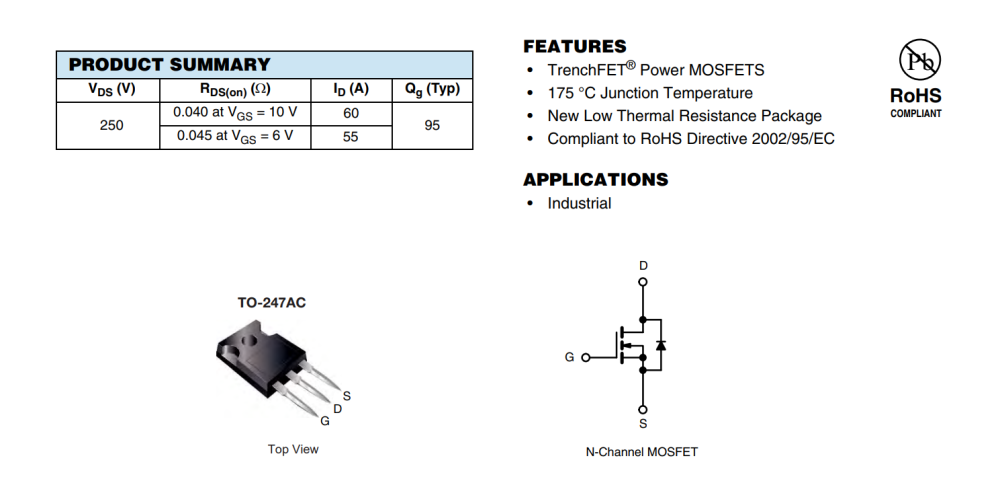
In the context of the current global energy transition, the utilization rate of renewable energy continues to increase. Clean energy such as solar and wind energy has become an important part of the energy structure. However, there are still challenges to the efficient conversion and storage of these renewable energy sources. VBP1254N MOSFETs were introduced by VBsemi because excellent performance and reliability were the key factors in solving these problems. High-efficiency inverter core The inverter is an important equipment that converts direct current into alternating current, and is widely used in solar power generation systems and wind power generation systems. The emergence of VBP1254N provides strong support for the efficient energy conversion of inverters. Its drain-to-source voltage (VDS) of 250V and drain-to-source current (ID) capability of 60A enable MOSFETs to handle high-power power conversion. In addition, VBP1254N uses advanced trench technology to provide low on-resistance (RDS(on)). When VGS=10V, the typical value is only 40mΩ. This feature significantly reduces energy loss, improves the conversion efficiency of the inverter, helps the system maintain low heat accumulation at high power output, and extends the life of the equipment. A reliable choice for battery management systems In renewable energy systems, battery management systems (BMS) are critical to the performance of energy storage devices. VBP1254N is a reliable choice for battery management systems due to its stable performance and high threshold voltage (Vth, 3.5V typical). MOSFETs can effectively control the current during charging and discharging to ensure the safe and efficient operation of the battery pack under different working conditions. Its ±20V gate-to-source voltage (VGS) feature enables VBP1254N to operate reliably under extreme conditions. This is particularly important for fast response and high reliability requirements in energy storage systems, ensuring that the system can quickly adjust the current under various load conditions, avoid overcharging or overdischarging the battery, and prolong the battery life. Application prospects and advantages The high performance of the VBP1254N makes it very promising for use in renewable energy systems. Whether it's an inverter or a battery management system, this MOSFET performs well. Its excellent performance in high-power energy conversion and energy storage applications perfectly overcomes the relevant technical difficulties and provides a solid guarantee for the efficiency and reliability of the energy system. Detailed parameter description 1. **Product model**: VBP1254N 2. **Package**: TO247 3. **Configuration**: Unipolar 4. **Polar**: N channel 5. **Drain-Source Voltage (VDS)**: 250V 6. **Gate-Source Voltage (VGS)**: ±20V 7. **Threshold voltage (Vth, typ)**: 3.5V 8. **On resistance (RDS(on)@VGS=10V, typ)**: 40mΩ 9. **Drain Current (ID)**: 60A 10. **Technology**: Trench 11. **Seamless replacement models**: IXTH50N25T, IRFP4229 Examples of other areas of application for the product 1. **Industrial Automation**: VBP1254N can be used for motor drives and control systems in industrial automation. Its high current handling capability and low on-resistance make it ideal for high-efficiency motor drives. Whether in factory automation equipment or robot control, the equipment provides reliable power transmission and stable performance. 2. Power Management:VBP1254N performs well in power management modules, especially in high-efficiency switching power supplies and DC-DC converters. Its low on-resistance and high threshold voltage ensure high efficiency and system stability for energy transfer, making it a high-efficiency power supplyA core component of the management system. High-performance devices designed to address high-power energy conversion and energy storageIssue. It not only improves the overall efficiency and stability of the renewable energy system, but also provides strong support for the further development of green energy. In the future, with the continuous progress of technology, VBP1254N will continue to give full play to its unique advantages in more fields to promote the innovation and application of energy technology.
-
- mosfet,
- semiconductors
-
(and 4 more)
Tagged with:
-
With the popularity of electric vehicles, smart grids are building compatible charging networks to achieve efficient distribution and management of energy. Smart grids that integrate traditional power grids with advanced communication technologies pave the way for building a more efficient, environmentally friendly and reliable energy system. RS485 repeaters can highly integrate modern advanced sensor measurement technology, communication technology, information technology, etc. with physical power grids, which helps to improve the management level, work efficiency, power grid reliability and service level of power companies. E810-R12/E810-R14/E810-R18 is an isolated repeater (HUB) for 1-channel RS485 to 2/4/8-channel RS485 launched by Ebyte. RS485 repeaters are communication devices that support 1-channel RS485 master device and 1-channel or multiple-channel RS485 slave devices. Photoelectric isolation technology is used to protect the master and slave devices from interference. No configuration is required, and transparent data transmission between the master and slave interfaces. RS485 Repeater Main features No packet loss Supports communication between one RS485 master device and one or more RS485 slave devices, and the slave communication port supports up to 32 nodes. The cached RS485 hub has a 5K cache per channel, and no packet loss. Multi-host gateway Multi-host gateway: allows multiple hosts or devices to communicate with the external network through the same gateway, which can adapt to more variable work requirements. E810-R41 and E810-R21 support multi-host gateway mode. Wide voltage power supply The power supply supports DC 9-40V wide voltage input, with overcurrent and reverse connection protection. Isolation + protection The communication and power supply between the master and slave interfaces are completely isolated, and the power supply signal between the host interface and the slave interface is completely isolated. The signal interface has static electricity, lightning strike, and surge protection. The circuit is designed according to the EMC level 3 standard, with 1.5KV isolation voltage, 4KV electrostatic protection contact discharge, 8KV air discharge, and 1KV differential mode and 2KV common mode lightning surge protection, which can effectively isolate the damage caused by lightning and static electricity to the equipment. High-speed transmission The host interface data can be sent to all slave interfaces at the same time, and the slave interface data can be sent to the host interface in time-sharing. Using super anti-interference and high-speed isolation devices, the baud rate can reach up to 230400bps. No configuration is required, it can be used immediately. Application scenarios This product is suitable for comprehensive RS485 communication systems such as automation control systems, monitoring systems, alarms, access control systems, IC card charging, meter reading, one-card pass, parking lot charging, etc. • Building automation and smart home In building automation systems, RS485 repeaters can be used to connect and manage various smart devices, such as thermostats, security systems, lighting controls, etc., to achieve centralized management and control. • Traffic management system In intelligent traffic systems, RS485 repeaters can be used to connect traffic lights, cameras, vehicle detectors and other equipment to achieve real-time monitoring and management of traffic flow. • Video surveillance system In large-scale video surveillance projects such as "Safe City", RS485 repeaters can ensure the accuracy and real-time nature of data transmission, especially in remote monitoring scenarios, they can ensure stable transmission of video data.


