-
Posts
11 -
Joined
-
Last visited
Contact Methods
-
Website URL
https://www.vbsemi.com/
vbsemi's Achievements
-
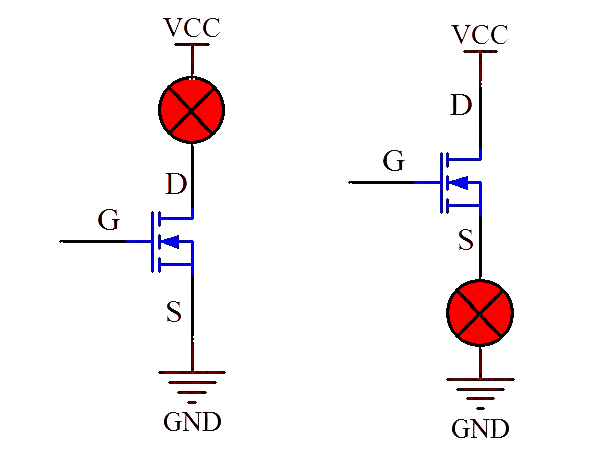
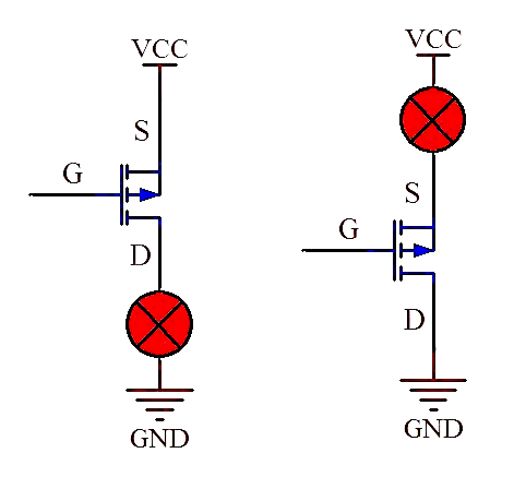
https://youtu.be/A7Q4pJbKY3k 有人说 NMOS 可以用作电路应用中的上管或下管。哪个更好?两者有什么区别? 众所周知,NMOS 和 PMOS 的电流方向相反,Vgs 具有一定的电压差。但是,NMOS 的 G 电位高于 S 电位 (5~10V),而 PMOS 的 S 电位高于 G 电位 (-5~-10V)。 这里,以 5V 的导通电压差为例,当使用 NMOS 作为下管时,S 极直接接地,将其固定到 5V 即可开启 G 极电压。 NMOS 如果用 NMOS 作为上管,D 极接正电源,S 极的电压不固定,则无法确定控制 NMOS 导通的 G 极电压,因为 S 极对地的电压有两种状态, MOS 管切断时为低电平,导通时接近高电平 VCC。但是,当 NMOS 用作上管时,控制电路会更加复杂。在这种情况下,必须使用隔离电源进行控制。改用 PMOS 会简单得多。 PMOS 使用 PMOS 作为上管时,S 极直接连接到电源 VCC,S 极电压是固定的,G 极电压只需要比 S 极低 5V 即可导通;同样,如果用 PMOS 作为下管,D 极接地, S 极电压不固定,无法确定控制极 G 极的电压,使用起来比较麻烦,需要隔离电压设计。 因此,在电路中通常使用 PMOS 作为上管,NMOS 作为下管。
-
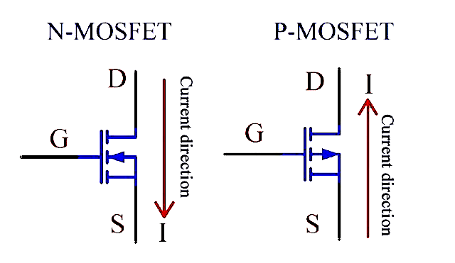
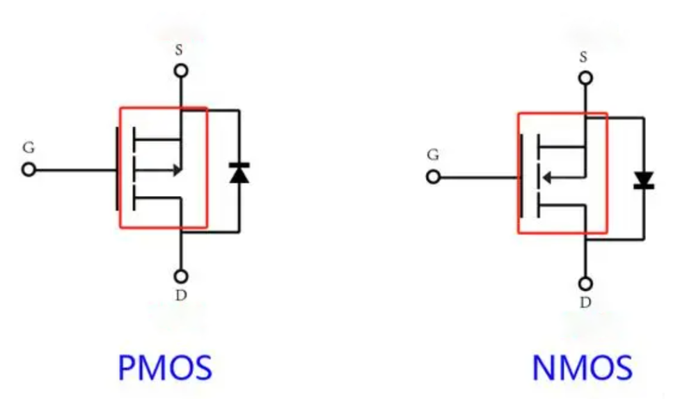
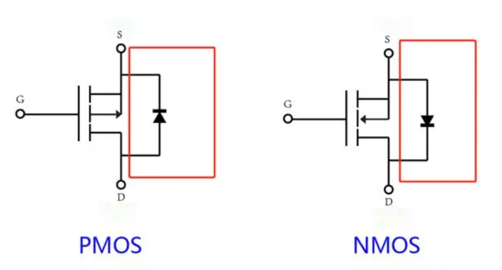
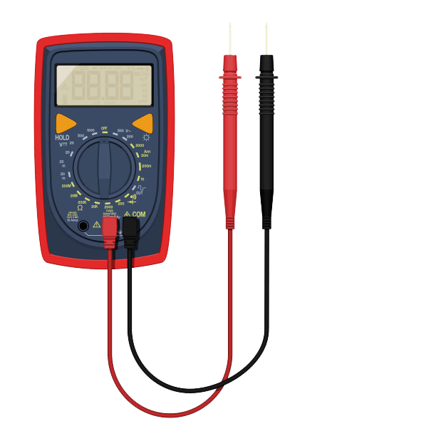
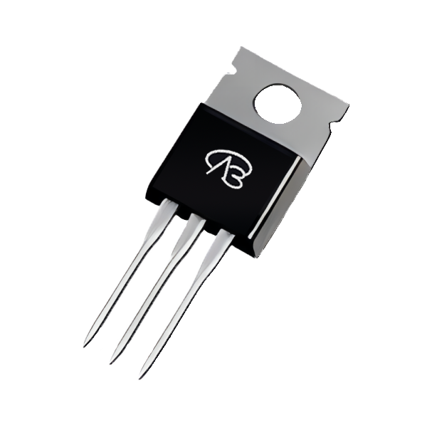
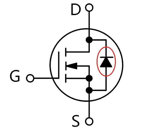
https://youtu.be/3e6fPoQ17wM 如何区分你手中的管子是N管还是P管? 首先,我们以增强MOS管为例。这是两者的电路符号: 您可以看到两个箭头的方向不一致。 这个箭头就是它的衬底,因为MOS管的内部衬底和源是连接在一起的。 NMOS和PMOS电路符号之间的最大区别在于其基板。NMOS的箭头指向闸门,而PMOS的箭头则指向闸门。 该箭头的方向与内部衬底与MOS管的通道逆温层之间的PN结方向有关。 其次,NMOS和PMOS的体二极管相反。 NMOS管的体二极管的阳极(即正极)连接到源极,PMOS的体二极管的阳极连接到漏极,体二极管的负极连接到源极。 那么,如何区分MOS管的三个引脚呢? 您可以使用万用表进行测试。下面简单说明一下。 拿一个封装为TO220的MOS管来说,它通常有一个散热片,散热片会连接到漏极。使用万用表测试哪个引脚可以连接到散热器,该散热器对应于漏极。 由于二极管的连接,漏极和源极之间存在二极管特性。 因此,当使用万用表测试漏极以及哪个引脚可以在正向和反向连接时,它就是源极。 剩下的就是大门了。 归纳起来,有两点: 1.NMOS二极管的正极一般接在源极上 2. 散热器连接到排水管
-
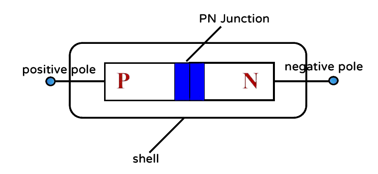
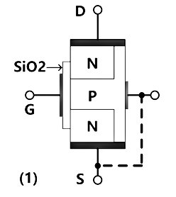
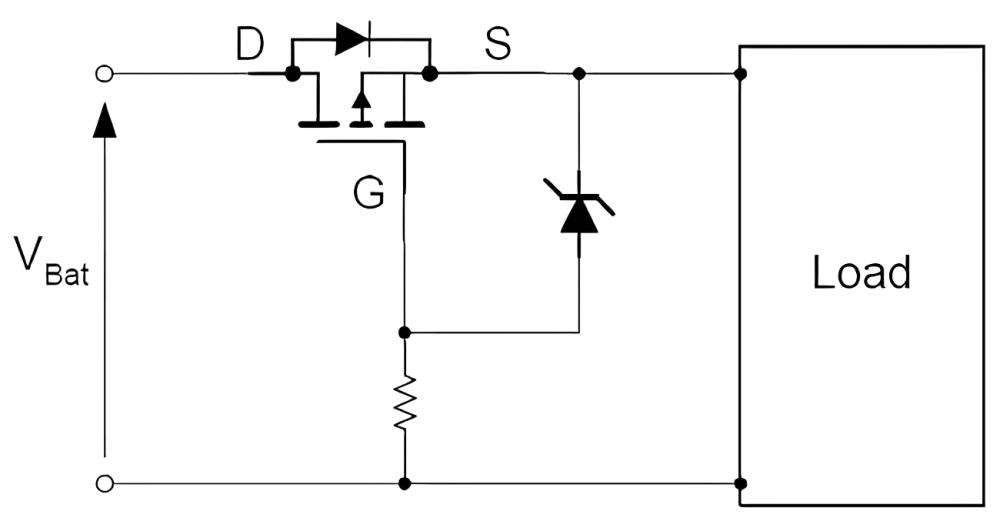
https://www.youtube.com/watch?v=pql2Ulae7mE MOS has a body diode connected in parallel between the D and S poles, so why is this diode connected in parallel? This starts with the process and structure of MOS. The diode is composed of a pair of PN junctions. The P-type region corresponds to the positive pole of the diode, the N-type region corresponds to the negative pole of the diode, and the PN junction is in the middle. SiO2 in the MOS tube itself is not conductive, so the driving pole G basically does not carry current. In addition to the three poles D, G, and S, there is also an intermediate pole, which is connected to the S pole, so in the circuit symbol of MOS, the arrow pointing to the channel N channel inside the MOS is connected to the S pole. In addition, the drain of the N-type region is connected to the middle P-type region and then to the source, which just forms a diode structure, so a diode is connected in parallel in the MOS symbol. What is the use of this body diode? In some scenarios, such as battery protection, after the lithium battery is over-discharged, the protection function will be turned on: turn off the discharge MOS. When the charger is plugged in, the MOS body diode is used to make the circuit conductive and the system work normally. However, in some scenarios, the existence of this diode is undesirable because it may cause leakage between the S pole and the D pole.
-

False Turn-On in MOSFET Driving Circuit and Countermeasures
vbsemi posted a topic in Theory articles
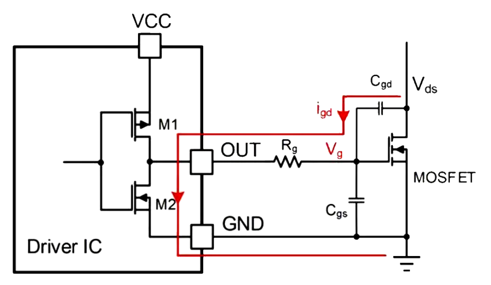
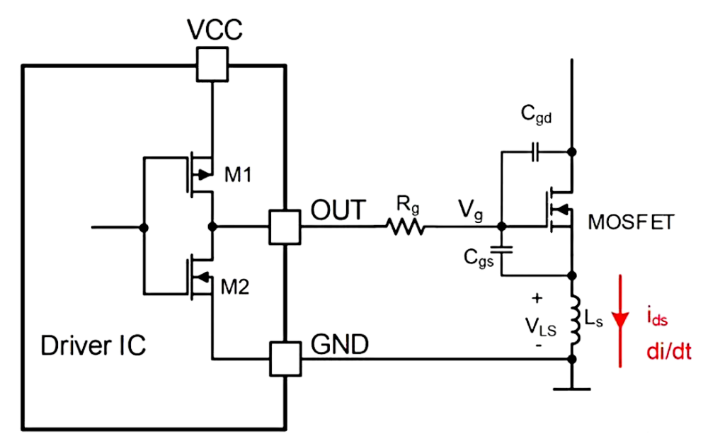
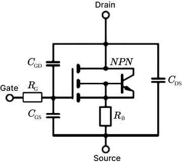
https://www.youtube.com/watch?v=PwOTTqUo9tA MOSFET is a switch controlled by gate voltage. When the gate voltage is greater than the turn-on threshold, the MOSFET is turned on; when the gate voltage is lower than the turn-on threshold, the MOSFET is turned off. In actual applications, due to the influence of other factors such as device and peripheral circuit parasitic parameters, the originally turned-off power device may be mistakenly turned on. Today, let's talk about the mistaken turn-on of MOSFET in the drive circuit and its countermeasures. Let's talk about two cases of mistaken turn-on: mistaken turn-on caused by Miller effect and mistaken turn-on caused by parasitic inductance. False turn-on caused by Miller effect When the MOSFET is turned off and then turned on, the Vds voltage (the maximum voltage that can be applied between the drain and the source) rises rapidly to produce a high dv/dt (the rate of change of the drain-source voltage during the switching transient), thereby generating a displacement current (igd) in the capacitor Cgd (Miller capacitor). This displacement current will generate a voltage spike after flowing through . If this voltage spike exceeds the turn-on threshold of the MOSFET, the MOSFET will be turned on, causing the circuit to be turned on or even damaged. Another type of false turn-on is caused by parasitic inductance on the line. As shown in the figure below, Ls is the parasitic inductance on the source of the MOSFET. When the MOSFET is turned off quickly, the current decreases rapidly to produce a high di/dt, and then a negative voltage (VLS) is generated across the two ends of the parasitic inductance. If this VLS voltage exceeds the gate threshold of the MOSFET, the MOSFET will be turned on by mistake. So, what methods do we have to deal with the phenomenon of MOSFET being turned on by mistake? 1. Adjust the gate drive resistor and capacitor The turn-on/off speed of the MOSFET can be adjusted by adjusting the size of the gate drive resistor and capacitor: increase the gate drive resistor and capacitor to slow down the turn-on/off speed of the MOSFET, reduce dv/dt (di/dt) and thus reduce the gate voltage spike. 2. Add a transistor A transistor can be placed near the gate of the power tube to prevent false opening during the shutdown period, effectively suppressing the false gate opening caused by the Miller effect. 3. Use an anti-parallel diode The current in the inductor can disappear through the diode loop, thereby avoiding the generation of reverse potential.-
- mosfet
- semiconductor
-
(and 2 more)
Tagged with:
-
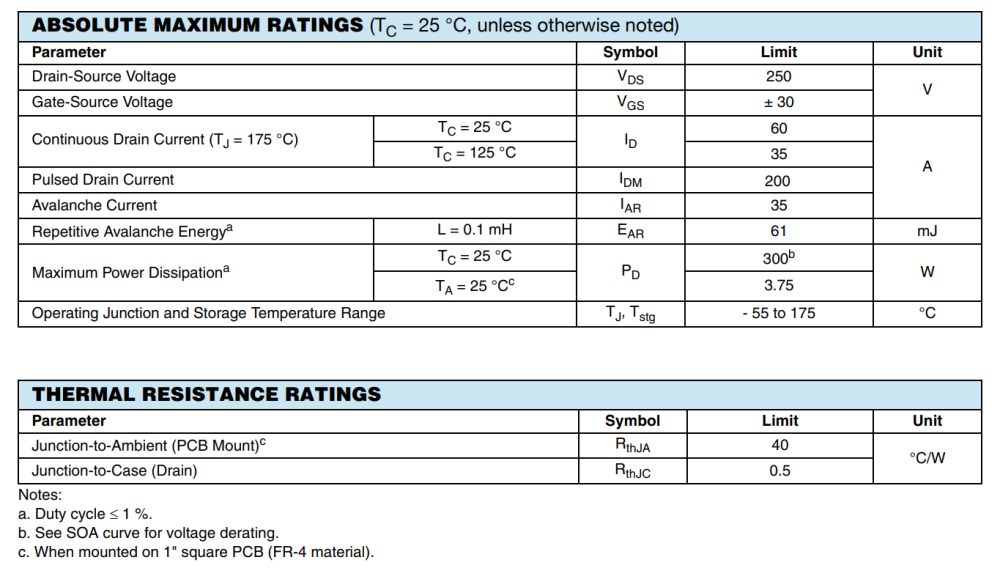
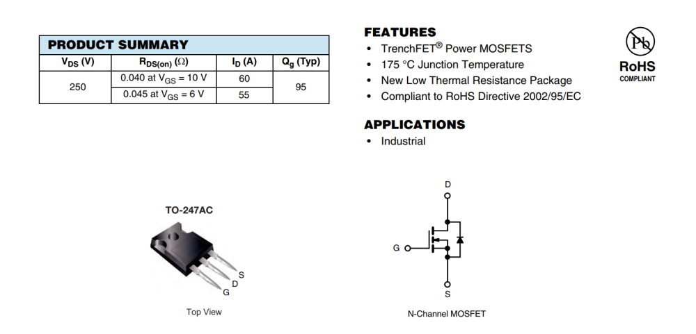
In the context of the current global energy transition, the utilization rate of renewable energy continues to increase. Clean energy such as solar and wind energy has become an important part of the energy structure. However, there are still challenges to the efficient conversion and storage of these renewable energy sources. VBP1254N MOSFETs were introduced by VBsemi because excellent performance and reliability were the key factors in solving these problems. High-efficiency inverter core The inverter is an important equipment that converts direct current into alternating current, and is widely used in solar power generation systems and wind power generation systems. The emergence of VBP1254N provides strong support for the efficient energy conversion of inverters. Its drain-to-source voltage (VDS) of 250V and drain-to-source current (ID) capability of 60A enable MOSFETs to handle high-power power conversion. In addition, VBP1254N uses advanced trench technology to provide low on-resistance (RDS(on)). When VGS=10V, the typical value is only 40mΩ. This feature significantly reduces energy loss, improves the conversion efficiency of the inverter, helps the system maintain low heat accumulation at high power output, and extends the life of the equipment. A reliable choice for battery management systems In renewable energy systems, battery management systems (BMS) are critical to the performance of energy storage devices. VBP1254N is a reliable choice for battery management systems due to its stable performance and high threshold voltage (Vth, 3.5V typical). MOSFETs can effectively control the current during charging and discharging to ensure the safe and efficient operation of the battery pack under different working conditions. Its ±20V gate-to-source voltage (VGS) feature enables VBP1254N to operate reliably under extreme conditions. This is particularly important for fast response and high reliability requirements in energy storage systems, ensuring that the system can quickly adjust the current under various load conditions, avoid overcharging or overdischarging the battery, and prolong the battery life. Application prospects and advantages The high performance of the VBP1254N makes it very promising for use in renewable energy systems. Whether it's an inverter or a battery management system, this MOSFET performs well. Its excellent performance in high-power energy conversion and energy storage applications perfectly overcomes the relevant technical difficulties and provides a solid guarantee for the efficiency and reliability of the energy system. Detailed parameter description 1. **Product model**: VBP1254N 2. **Package**: TO247 3. **Configuration**: Unipolar 4. **Polar**: N channel 5. **Drain-Source Voltage (VDS)**: 250V 6. **Gate-Source Voltage (VGS)**: ±20V 7. **Threshold voltage (Vth, typ)**: 3.5V 8. **On resistance (RDS(on)@VGS=10V, typ)**: 40mΩ 9. **Drain Current (ID)**: 60A 10. **Technology**: Trench 11. **Seamless replacement models**: IXTH50N25T, IRFP4229 Examples of other areas of application for the product 1. **Industrial Automation**: VBP1254N can be used for motor drives and control systems in industrial automation. Its high current handling capability and low on-resistance make it ideal for high-efficiency motor drives. Whether in factory automation equipment or robot control, the equipment provides reliable power transmission and stable performance. 2. Power Management:VBP1254N performs well in power management modules, especially in high-efficiency switching power supplies and DC-DC converters. Its low on-resistance and high threshold voltage ensure high efficiency and system stability for energy transfer, making it a high-efficiency power supplyA core component of the management system. High-performance devices designed to address high-power energy conversion and energy storageIssue. It not only improves the overall efficiency and stability of the renewable energy system, but also provides strong support for the further development of green energy. In the future, with the continuous progress of technology, VBP1254N will continue to give full play to its unique advantages in more fields to promote the innovation and application of energy technology.
-
- mosfet,
- semiconductors
-
(and 4 more)
Tagged with:
-
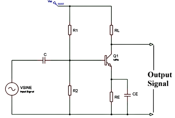
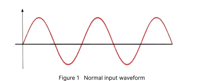
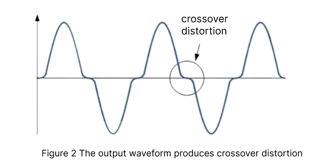
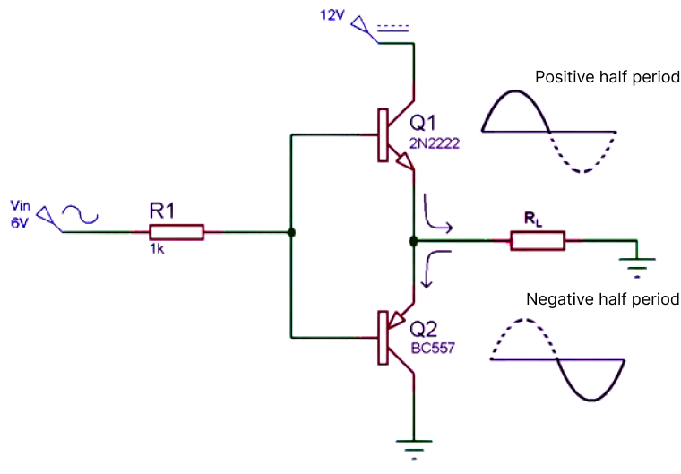
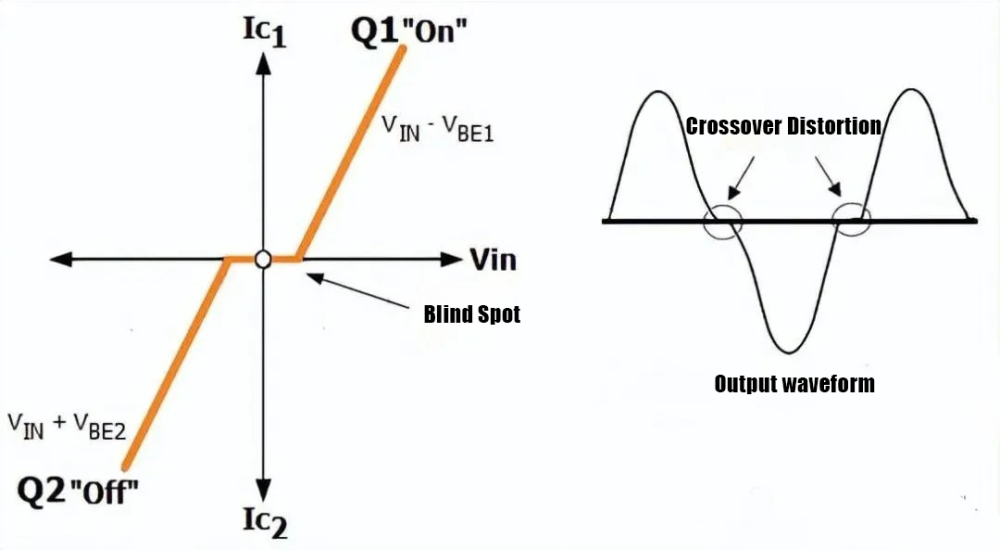
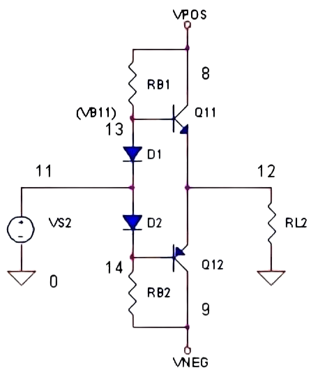
We know that push-pull circuits come in many types, such as class A or class B amplifiers. Class B amplifiers are the ones used in practical applications. They are more efficient than class A, but they are often affected by crossover distortion. So how does it affect it? How can it be reduced? When the signal is distorted at 0V, the transistor will provide a voltage of 0.7v at the base-emitter junction before turning on. When the AC input voltage is applied to the push-pull amplifier, it increases from 0 until it reaches 0.7V, and the transistor remains off without any output. So why does crossover distortion occur when VIN reaches zero? (Class B amplifier) In fact, transistors Q1 and Q2 cannot be turned on at the same time. If Q1 is turned on, VIN must be greater than Vout, and if Q2 is turned on, Vin must be less than Vout. If VIN is equal to zero, Vout must also be equal to zero. When VIN increases from zero, the output voltage Vout will also remain at zero. Until V IN is less than 0.7V, the output voltage shows a dead zone, and the same situation will occur when V IN starts to decrease from zero. How to reduce the crossover distortion of the push-pull transistor circuit? It can be corrected by using two diodes that are turned on at the transistor position, that is, the class AB amplifier circuit. It uses the characteristics of both. From 0V to 0.7V, the diode is biased in the on state to make up for the 0.7 V loss of the emitter follower. At this time, the transistor has no signal at the base, which solves the crossover distortion problem. In addition, it can also be achieved by reducing the resistance value. This is because the resistor RB1 controls the current of D1. The smaller RB1 is, the greater the current is, that is, the greater the voltage of the diode is, so when there is no input signal, the Vbe will be greater. This increased deviation will further reduce the distortion. However, the specific application situation is still based on the actual circuit design.
-
- mosfet
- semiconductor
- (and 4 more)
-
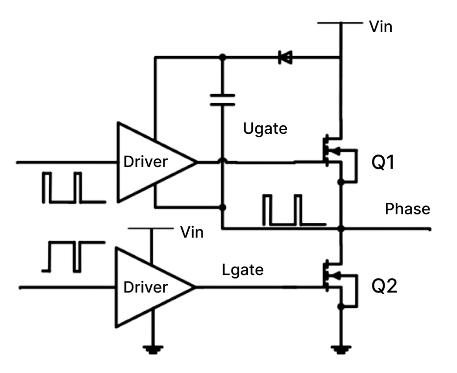
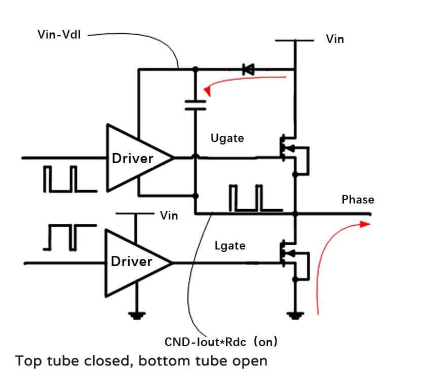
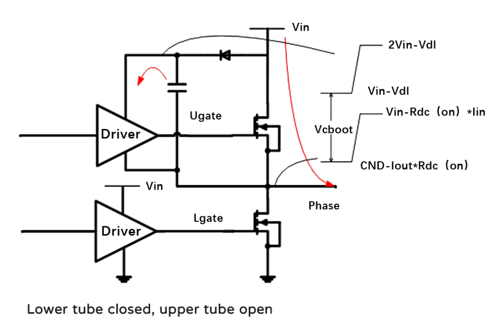
We know that the Buck circuit generally needs a "top tube" to control it, and this realization of raising its own voltage mainly depends on a capacitor, which is the bootstrap capacitor. So how does this capacitor achieve its function? For example, a small capacitor is connected between the GS of the MOS. The MOS charges the capacitor when it is not turned on. When the MOS is turned on, when the S-pole voltage increases, the power supply voltage of the driver above will be automatically increased. At this time, the output voltage of the driver also increases and is connected to the G-pole of the top tube. In other words, the G-pole generates high voltage, and there is enough voltage difference Vgs between the G-pole and the S-pole, so the top tube MOS continues to be turned on. During the charging process, the IC will prohibit the upper and lower tubes from being turned on at the same time to prevent direct conduction. In other words, the upper tube will be turned off and the lower tube will be turned on, and then the diode D1 and the bootstrap capacitor C1 will form a charging circuit. The input power passes through D1, C1, the lower tube, and finally to the ground (negative pole of the power supply), forming a loop to charge the capacitor so that the voltage on both sides of the capacitor is equal to the input power. Conversely, when the lower tube is turned off, the previous loop is naturally cut off, and D1 is in reverse cutoff. At this time, the capacitor will keep the voltage change continuous, and the Vc voltage will gradually decrease with discharge without sudden changes. However, during the charging process, since the capacitor has been charged, the Vc voltage is approximately Vin, so the Vgs of the upper tube is also equal to the input power supply, and this voltage is enough to turn on the upper tube. In this way, a PWM cycle is completed, which is the charging and discharging process of the bootstrap capacitor.
-
VBsemi is proud to introduce the new TO220 package VBM115MR03 designed specifically for high-voltage applications. With its excellent performance and reliability, this product has become an ideal alternative to traditional high-voltage products. Excellent performance: Ultra-high withstand voltage: The VBM115MR03 design supports voltages up to 1500V to ensure stable operation in harsh high-voltage environments and ensure the safety and reliability of the system. Very low on-resistance: The low on-resistance of only 6000 milliohms effectively reduces energy consumption and heat dissipation requirements, improves system efficiency, and extends equipment life. Powerful current-carrying capacity: The maximum current reaches 3A, allowing VBM115MR03 to easily handle the high load requirements in most industrial and consumer electronics applications and ensure stable operation. With its excellent performance, VBM115MR03 has become the first choice for engineers designing high-voltage circuits. It is widely used in industrial automation, power conversion, medical equipment, electric vehicle charging systems, and other fields, with extraordinary reliability and capability. Benefits & Highlights: Wide compatibility: VBM115MR03 has excellent compatibility and can directly replace a variety of high-voltage products, including but not limited to IRFBG30, SiHFBG30, IXTP3N120, etc., providing engineers with greater flexibility and choice. Stable and reliable: After strict quality control and comprehensive performance testing, it ensures that the VBM115MR03 maintains stable electrical performance and reliability in long-term use, reducing maintenance costs and risks. Diverse applications: VBM115MR03 are widely used in key fields such as industrial control systems, power converters, medical equipment, and electric vehicle charging systems, providing efficient and reliable solutions for various application scenarios. With these advantages, VBM115MR03 stands out in high-voltage circuit design and is ideal for engineers to choose a reliable solution. Apply: VBM115MR03 is widely used in many key areas, including but not limited to the following: Industrial automation control system: In industrial automation, VBM115MR03 is the core component of motor drive, power management and electrical control system to ensure the reliable operation of equipment in high-voltage environments. Power conversion and inverter: As a key component of power converters and inverters, VBM115MR03 can efficiently convert and manage electrical energy, and are suitable for solar inverters, grid-connected and off-grid energy systems, ensuring stable and efficient energy conversion. Medical devices: In medical devices, VBM115MR03 are used for high-voltage power management, precision control circuits, electrical isolation, etc., to ensure the safe operation and precise control of medical devices, including imaging equipment, surgical instruments, and monitoring equipment. EV Charging Systems: VBM115MR03 EV charging systems provide charging efficiency and circuit safety, support fast charging and long-term use, and meet the stringent requirements of the EV market for efficient energy management and reliability. VBM115MR03.pdf
-
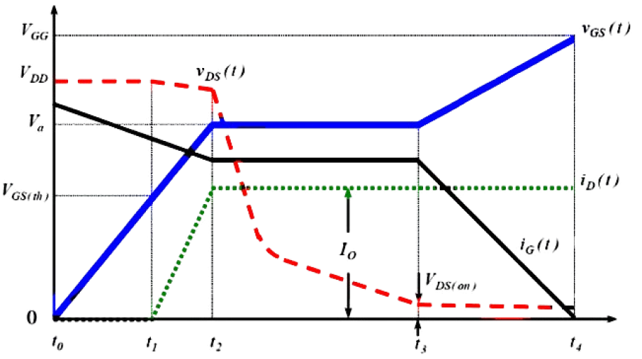
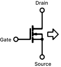
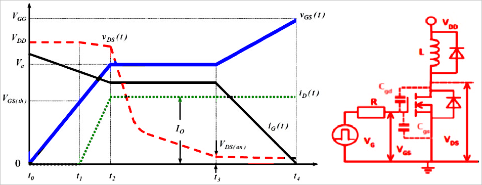
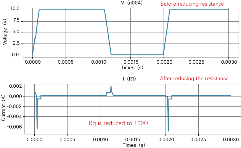
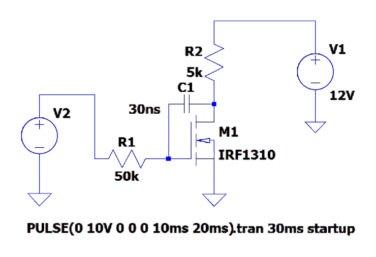
In some high-frequency switching circuits, the Miller effect of MOS tubes has the unpleasant disadvantages of extending the switching frequency, increasing power consumption, and reducing system stability. As shown in the figure below, there is a small flat step between t2 and t3, and the blue straight line part is the "Miller platform". MOS tube conduction (Miller effect): When MOSFET is turned on, Vds starts to drop and Id starts to rise, at which time MOSFET enters the saturation region; but due to the Miller effect, Vgs will not rise for a period of time, at which time Id has reached the maximum, and Vds continues to drop until the Miller capacitor is fully charged, and Vgs rises to the value of the driving voltage. At this time, MOSFET enters the resistance region, at which time Vds drops completely and the turn-on ends. Miller effect: Since the Miller capacitor prevents the rise of Vgs, it also prevents the fall of Vds, which will prolong the loss time and increase the loss. The left figure below is the circuit symbol diagram of the MOS tube, and the right figure is the equivalent model of the MOS tube. Miller capacitance shown in the figure Cgs: GS parasitic capacitance Cgd: GD parasitic capacitance Input capacitance Ciss = Cgs + Cgd Output capacitance Coss = Cgd + Cds Reverse transfer capacitance Crss = Cgd Miller effect refers to the effect of the equivalent input capacitance value being amplified by the distributed capacitance Cgs between the input and output under the effect of inverting amplification. The Miller effect will form a Miller platform. Disadvantages of Miller effect: From the first figure, we can see that under inductive load, the switching process of the MOS tube is significantly prolonged due to the Miller effect. The longer the D and S poles of the MOS tube overlap, the greater the conduction loss will be. Miller capacitance is bound to exist due to the manufacturing process of MOS tubes, so it cannot be completely eliminated. However, we can reduce the impact of the Miller effect by reducing the gate resistance Rg. It can be seen that the smaller R1 is, the faster gs is charged and the faster the MOS tube is turned on. However, is the Miller effect really useless? We know that everything has two sides, and the existence of the Miller effect is bound to be so. We can use the Miller effect to achieve the purpose of slow start of the circuit. By increasing the gate resistance of the MOS tube and connecting a large capacitor in parallel between the G-D poles of the MOS tube, the Miller step can be artificially lengthened. The circuit in the figure below increases the parallel capacitance between the gate resistance and the G-D pole, increases the Miller step, and turns the output waveform into a triangular pulse.
-
vbsemi changed their profile photo
-
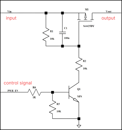
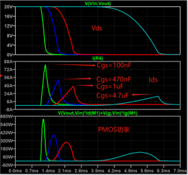
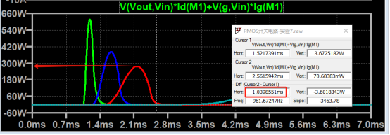
提到MOS管烧毁,一般是因为它非工作在SOA工作区,还有一种情况就是MOS管过流了。 比如这个电路中PMOS管最大允许的电流是50A,在MOS管开启瞬间最大电流达到了80+,那这个电流就非常大了。 此时的PMOS属于超规格使用了,我们可以在SOA曲线上看出,它并没有工作在SOA区间,这将会导致PMOS损坏。 那如果选择更高电流的PMOS呢?当然可以,但是成本会更高。 我们可以选择调节下外围电阻或者电容,让PMOS开通的速度更慢,这样电流就可以降下来。 比如调整R1,R2,还有gs之间的跨接电容,当Cgs调整为1uF时,Ids最大只有40A,在电流方面这就可以了,并且满足了80%的降额。 (50安培*0.8=40安培) 接下来我们看功率方面,从SOA曲线上看,MOS管的开通时间约为1ms,此时的最大功率是280W。 芯片正常热阻是50°C/W,最高结温可以是302°F。 假设环境温度是77°F,那么1ms能承受的瞬间功率大概在357W。 这里的 PMOS实际功率在280W,并没有超过限制,也就是说它正常工作在SOA区。 因此,当MOS管开通瞬间电流冲击较大时,可以适当调整Cgs电容,让PMOS 工作在SOA区,就可以避免MOS损坏的问题了。
-
- mosfet
- overcurrent,
-
(and 1 more)
Tagged with:


