
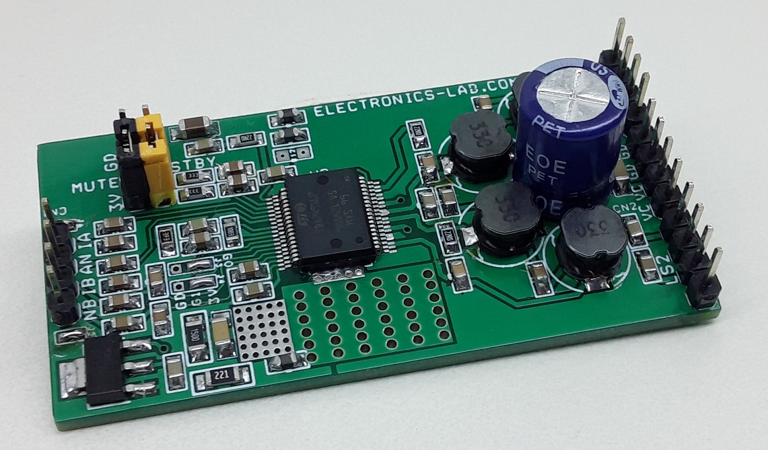
5 W + 5 W Dual BTL Class-D Audio Amplifier
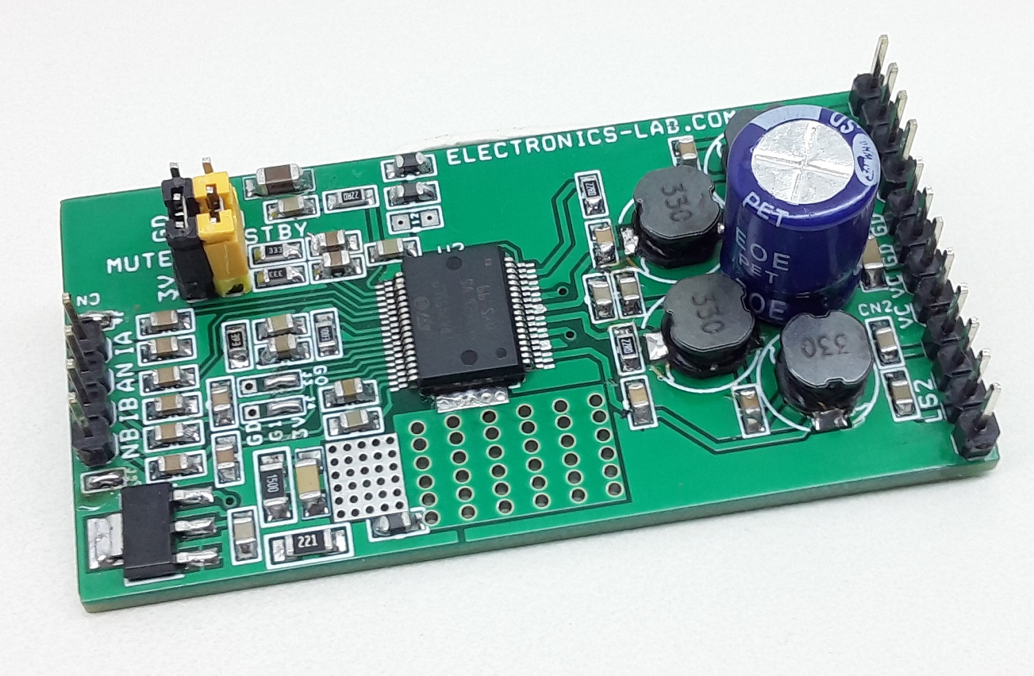
The project described here is a high-efficiency dual BTL class-D audio amplifier with single supply operations. The project was built using TDA7491LP13TR from ST. The low profile PCB design can fit in a small area, operating power supply 9-12V DC, Project supports single-ended or differential audio signal inputs. Jumpers are provided to set the various gains, standby, and mute functions.
Key Features
- 5W + 5W Continuous Output Power, 10% THD, (8 Ohms Speaker) at 9V DC
- Single Supply Operation 9V to 12V
- Four Selectable Fixed Gains Settings of nominally 20dB, 26dB, 30dB, 32dB Using Jumpers
- Differential Inputs Minimize Common-Mode Noise
- Jumper for Single-Ended Inputs
- No “Pop” Sound at Turn-On/Off
- Thermal Over Load Protection
- Standby and Mute Features Using Jumpers
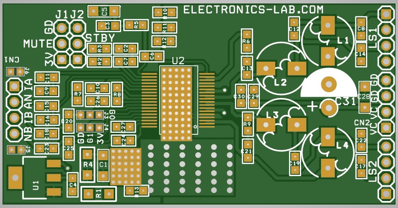
- PCB Dimensions 63.25 x 32.39 mm
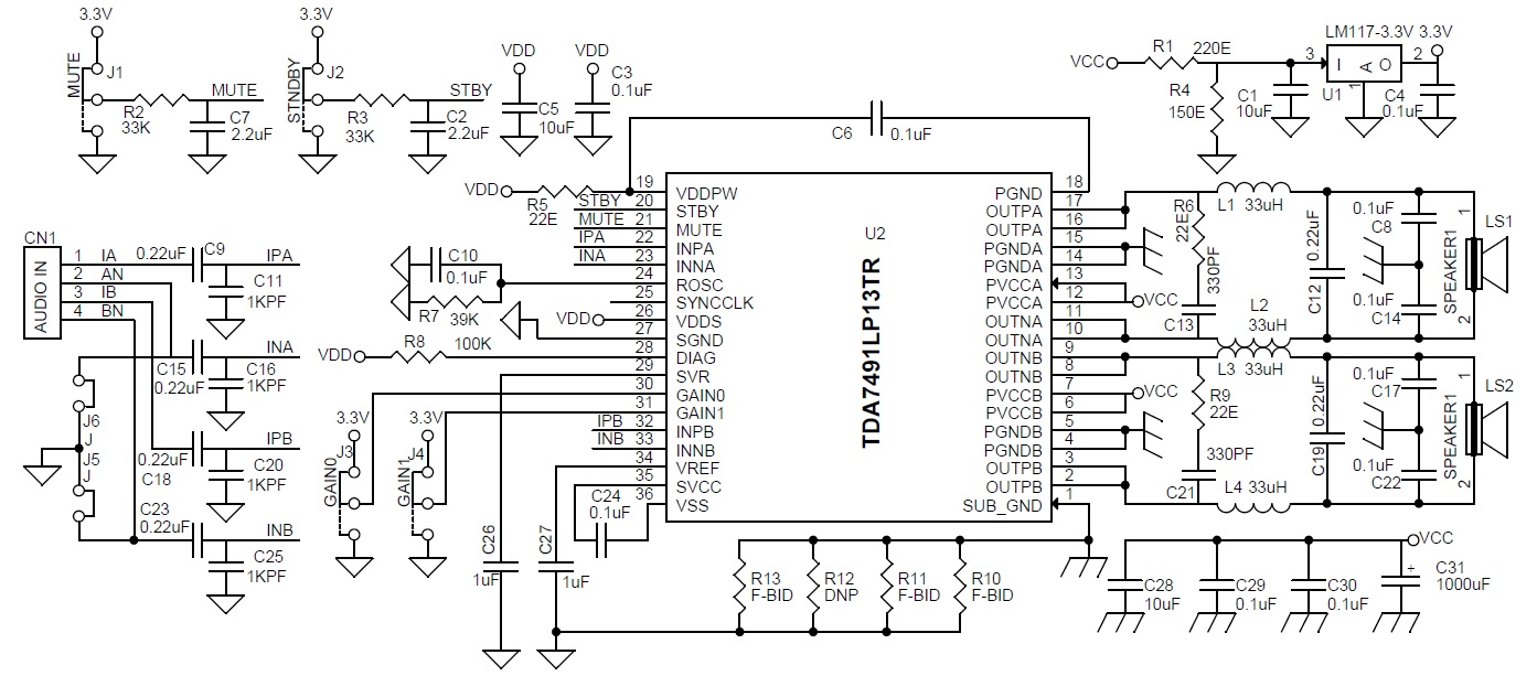
Mode Selection
There are three operating modes defined bellow:
- Standby mode: all circuits are turned off, very low current consumption
- Mute mode: inputs are connected to the ground and the positive and negative PWM outputs are at 50% duty cycle.
- Play mode: the amplifiers are active
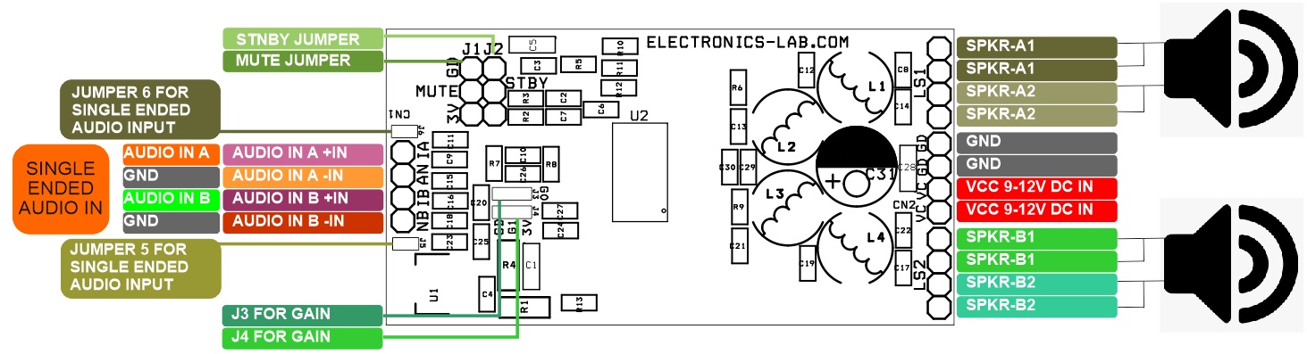
Jumper Setting Standby, Mute and Play Mod (Low=GND, High=3.3V)
- Standby Mode: Jumper J2 =Low, Jumper J1 (Don’t Care Whether low or high)
- Mute Mode: Jumper J2=High, Jumper J1 Low
- Play Mode: Jumper J2 = High, Jumper J1 High
Audio Signal Input (Single-Ended or Differential) Differential audio signal can be feed directly to CN1 , PIN 1 to 4
- Pin 1 >> IA +Input A Channel, Pin 2>> AN -Input A Channel
- Pin 3 >> NB +Input B Channel, Pin 4>> BN -Input B Channel
- For Single Ended Input Solder Jumper J5 and J6 (Channel A Input Pin1 Signal and Pin 2 GND, Channel B Pin3 Signal and Pin 4 GND)
Gain Setting (PCB Solder Jumper J3 and J4)
The gain of the TDA7491LP is set by the two inputs, GAIN0 (pin 30) and GAIN1 (pin 31). Internally, the gain is set by changing the feedback resistors of the amplifier.
- J3>>Low, J4>>Low =20dB (High=3.3V, Low=GND)
- J3>>Low, J4>>High =26dB (High=3.3V, Low=GND)
- J3>>High, J4>>Low =30dB (High=3.3V, Low=GND)
- J3>>High, J4>>High =32dB (High=3.3V, Low=GND)
Schematic
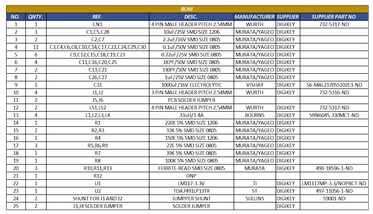
Parts List
| NO. | QNTY. | REF. | DESC. | MANUFACTURER | SUPPLIER | SUPPLIER PART NO |
|---|---|---|---|---|---|---|
| 1 | 1 | CN1 | 4 PIN MALE HEADER PITCH 2.54MM | WURTH | DIGIKEY | 732-5317-ND |
| 2 | 3 | C1,C5,C28 | 10uF/25V SMD SIZE 1206 | MURATA/YAGEO | DIGIKEY | |
| 3 | 2 | C2,C7 | 2.2uF/16V SMD SIZE 0805 | MURATA/YAGEO | DIGIKEY | |
| 4 | 11 | C3,C4,C6,C8,C10,C14 | 0.1uF/50V SMD SIZE 0805 | MURATA/YAGEO | DIGIKEY | |
| C17,C22,C24,C29,C30 | 0.1uF/50V SMD SIZE 0805 | MURATA/YAGEO | DIGIKEY | |||
| 5 | 6 | C9,C12,C15,C18,C19,C23 | 0.22uF/25V SMD SIZE 0805 | MURATA/YAGEO | DIGIKEY | |
| 6 | 4 | C11,C16,C20,C25 | 1KPF/50V SMD SIZE 0805 | MURATA/YAGEO | DIGIKEY | |
| 7 | 2 | C13,C21 | 330PF/50V SMD SIZE 0805 | MURATA/YAGEO | DIGIKEY | |
| 8 | 2 | C26,C27 | 1uF/25V SMD SIZE 0805 | MURATA/YAGEO | DIGIKEY | |
| 9 | 1 | C31 | 1000uF/16V ELECTROLYTIC | VISHAY | DIGIKEY | 56-MAL217055102E3-ND |
| 10 | 4 | J1,J2 | 3 PIN MALE HEADER PITCH 2.54MM | WURTH | DIGIKEY | 732-5316-ND |
| 11 | 2 | J5,J6 | PCB SOLDER JUMPER | |||
| 12 | 2 | LS1,LS2 | 4 PIN MALE HEADER PITCH 2.54MM | WURTH | DIGIKEY | 732-5317-ND |
| 13 | 4 | L1,L2,L3,L4 | 33uH/1.4A | BOURNS | DIGIKEY | SRN6045-330MCT-ND |
| 14 | 1 | R1 | 220E 5% SMD SIZE 1206 | MURATA/YAGEO | DIGIKEY | |
| 15 | 2 | R2,R3 | 33K 5% SMD SIZE 0805 | MURATA/YAGEO | DIGIKEY | |
| 16 | 1 | R4 | 150E 5% SMD SIZE 1206 | MURATA/YAGEO | DIGIKEY | |
| 17 | 3 | R5,R6,R9 | 22E 5% SMD SIZE 0805 | MURATA/YAGEO | DIGIKEY | |
| 18 | 1 | R7 | 39K 5% SMD SIZE 0805 | MURATA/YAGEO | DIGIKEY | |
| 19 | 1 | R8 | 100K 5% SMD SIZE 0805 | MURATA/YAGEO | DIGIKEY | |
| 20 | 3 | R10,R11,R13 | FERRITE-BEAD SMD SIZE 0805 | MURATA | DIGIKEY | 490-18596-1-ND |
| 21 | 1 | R12 | DNP | |||
| 22 | 1 | U1 | LM117-3.3V | TI | DIGIKEY | LM1117MP-3.3/NOPBCT-ND |
| 23 | 1 | U2 | TDA7491LP13TR | ST | DIGIKEY | 497-11056-1-ND |
| 24 | 2 | SHUNT FOR J1 AND J2 | JUMPPER SHUNT | SULLINS | DIGIKEY | S9001-ND |
| 25 | 2 | J3,J4 SOLDER JUMPER | SOLDER JUMPER | DIGIKEY |
Connections
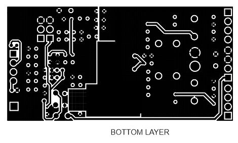
Gerber View
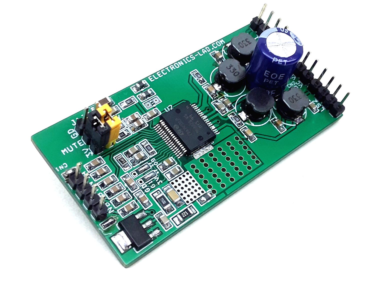
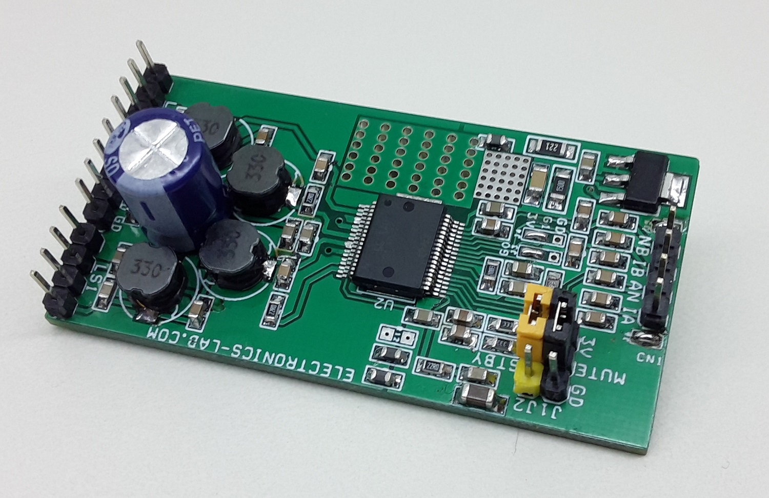
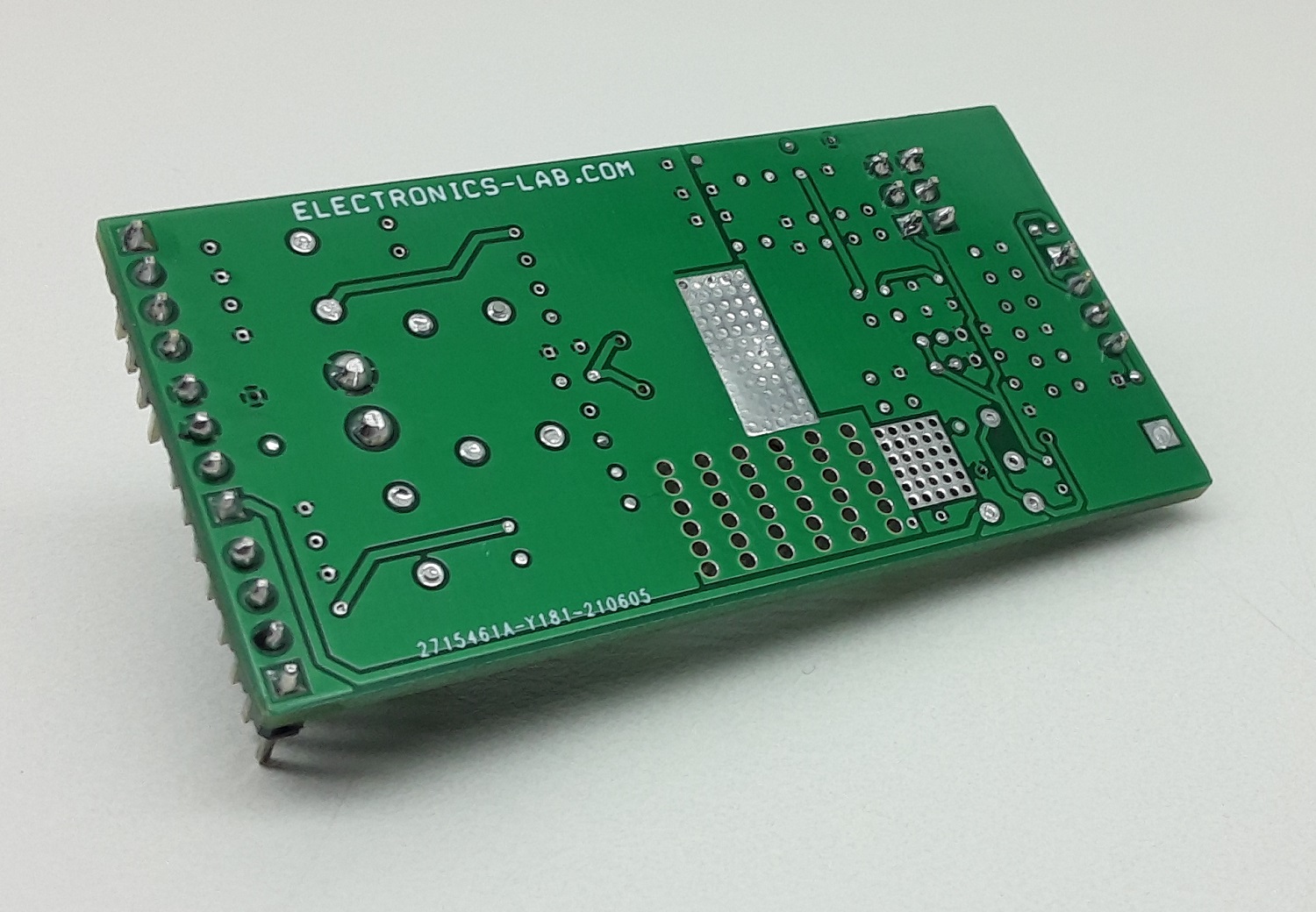
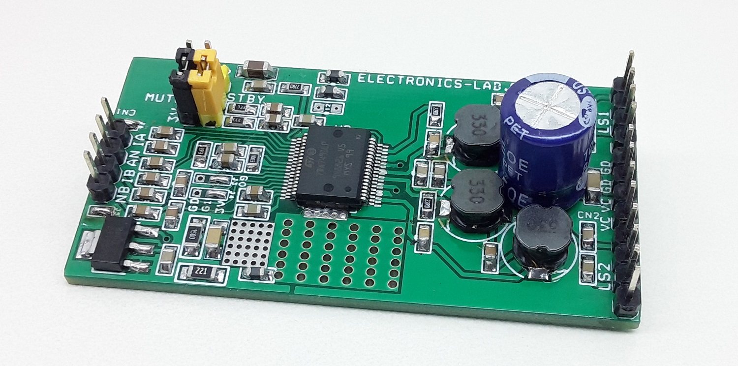
Photos
Video
TDA7491LP13TR Datasheet
Please follow and like us:
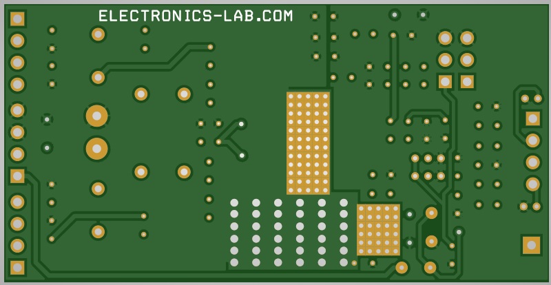
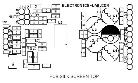
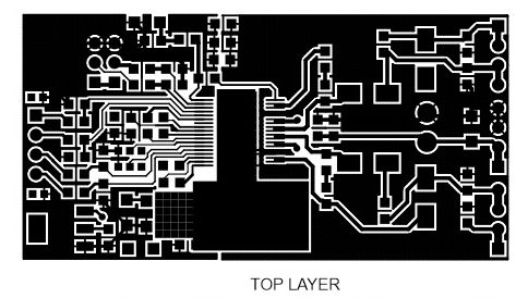
PCB


Subscribe
Login
0 Comments